

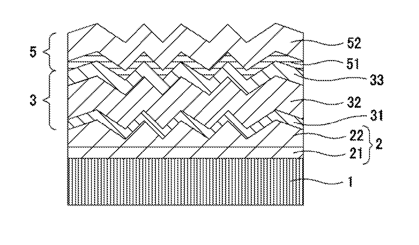
Transparent-conductive-film laminate, manufacturing method therefor, thin-film solar cell, and manufacturing method therefor
a technology of transparent conductive film and manufacturing method, which is applied in the direction of sustainable manufacturing/processing, final product manufacturing, vacuum evaporation coating, etc., can solve the problems of poor transparency, loss of film transparency, and preventing the realization of thin-film solar cells having high conversion efficiency, etc., to achieve excellent conductivity and cost reduction, excellent optical confinement effect, and excellent effect of optical confinemen
- Summary
- Abstract
- Description
- Claims
- Application Information
AI Technical Summary
Benefits of technology
Problems solved by technology
Method used
Image

Examples
example 1
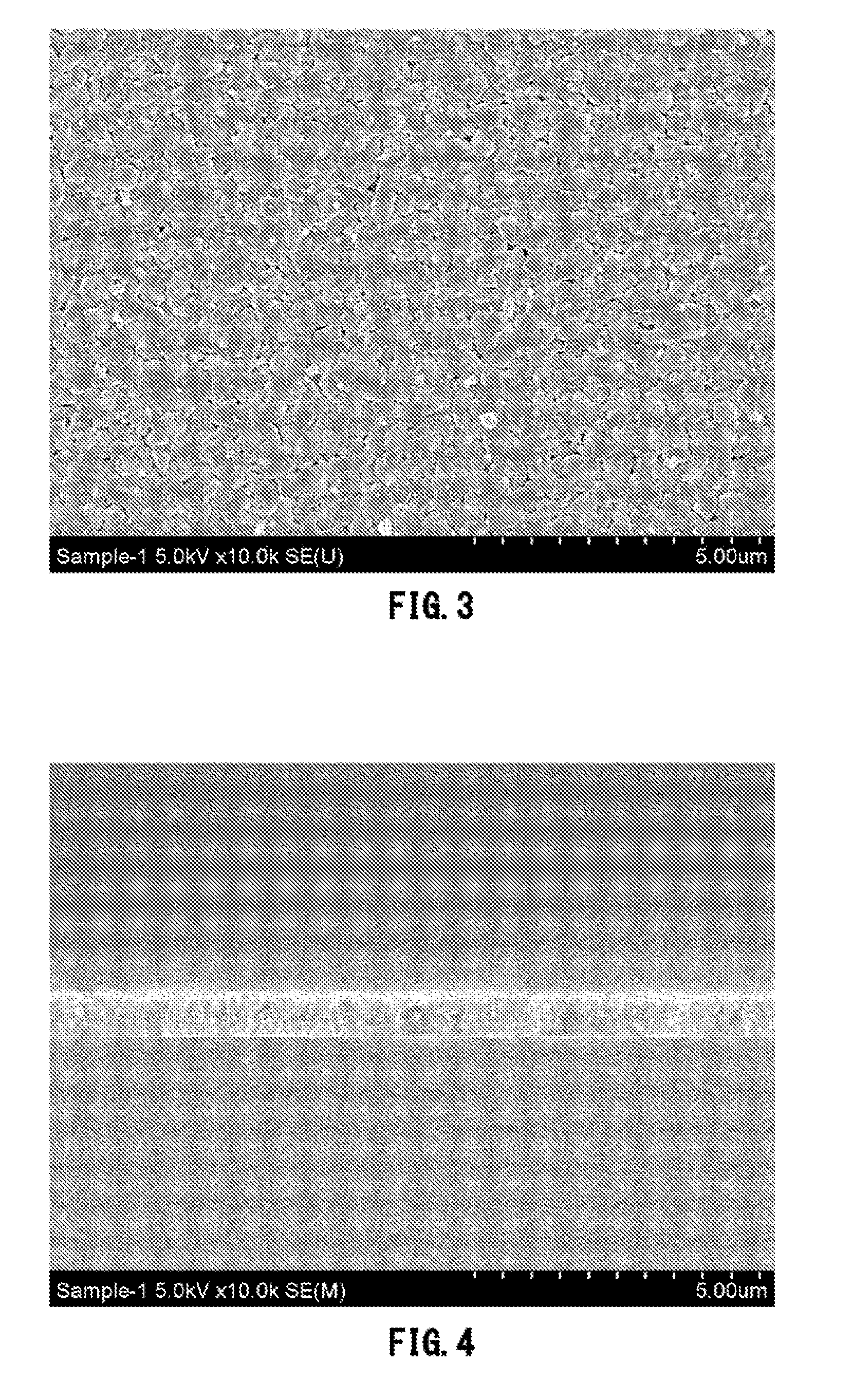
[0127]Using the following procedure, a zinc-oxide-based transparent conductive film (II) was laminated on an indium-oxide-based transparent conductive film (I) containing titanium (Ti) to prepare a transparent-conductive-film laminate with high surface-roughness.
[0128](Preparation of indium-oxide-based transparent conductive film (I))
[0129]First, under the conditions listed in the following Table 1, an indium-oxide-based transparent conductive film (I) to serve as a ground was deposited. The composition of a target (manufactured by Sumitomo Metal Mining Co., Ltd.) used for preparation of the indium-oxide-based transparent conductive film (I) was quantitatively analyzed using the foregoing method (1), and, as a result, it was found that the target had an atomic number ratio Ti / (In+Ti) of 0.50 atom %. Furthermore, the target had a purity of 99.999% and a size of 6 inches in diameter and 5 mm in thickness.
[0130]This sputtering target was attached to a cathode for ferromagnetic targets ...
example 2
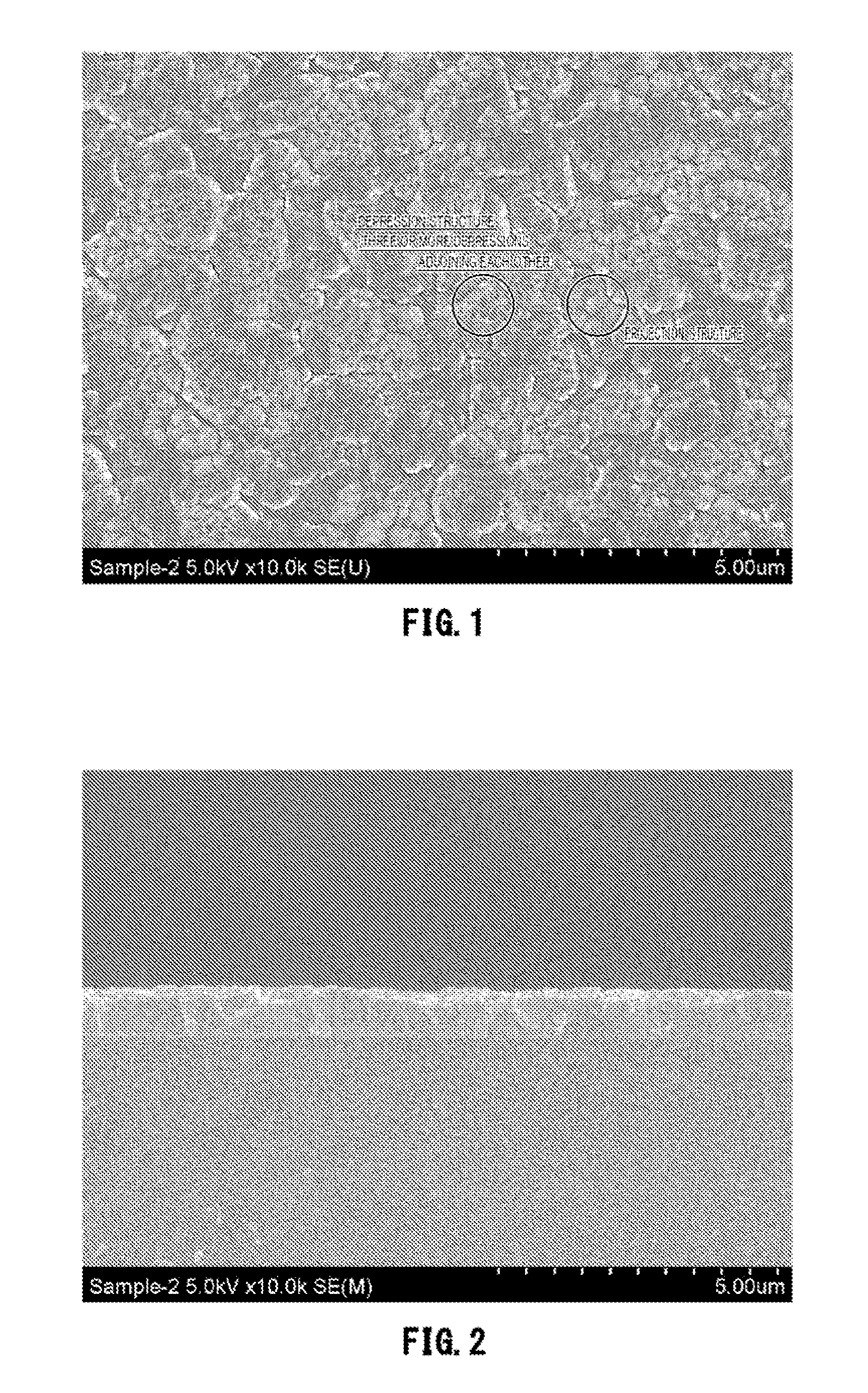
Comparative Example 1
[0140]Transparent-conductive-film laminates were prepared and the characteristics thereof were measured and evaluated in the same manner as in Example 1, except that the substrate temperatures at the time of deposition of the indium-oxide-based transparent conductive films (I) were 50° C. (Example 2) and 100° C. (Comparative Example 1), respectively.
[0141]The following Table 2 shows the obtained results. As shown in Table 2, in Comparative Example 1, the indium-oxide-based transparent conductive film (I) had an orientation only in the plane (222) of an In2O3 phase. Consequently, when the orientation of a ZnO layer was evaluated by X-ray diffraction after the lamination of the zinc-oxide-based transparent conductive film (II), the diffraction peak of the (002) plane was detected, but the diffraction peak of the (101) plane was not detected. Furthermore, as a result of evaluating the rocking curve of the (002) plane of ZnO hexagonal crystals, the inclination of th...
examples 3 and 4
Comparative Examples 2 and 3
[0144]Transparent-conductive-film laminates were prepared and the characteristics thereof were measured and evaluated in the same manner as in Example 1, except that the indium-oxide-based transparent conductive films (I) had a film thickness of 0 nm (no film) (Comparative Example 2), 10 nm (Example 3), 250 nm (Example 4), and 350 nm (Comparative Example 3), respectively.
[0145]The following Table 2 shows the obtained results. As shown in Table 2, in Comparative Example 2, an indium-oxide-based transparent conductive film (I) was not provided, whereby, when the orientation of a ZnO layer was evaluated by X-ray diffraction, the diffraction peak of the (002) plane was detected, but the diffraction peak of the (101) plane was not detected. Furthermore, rocking curve evaluation of the (002) plane of ZnO hexagonal crystals revealed that there was no inclination of the (002) plane.
[0146]Next, observations of the surface structure of the obtained transparent-cond...
PUM
| Property | Measurement | Unit |
|---|---|---|
| Temperature | aaaaa | aaaaa |
| Temperature | aaaaa | aaaaa |
| Temperature | aaaaa | aaaaa |
Abstract
Description
Claims
Application Information