

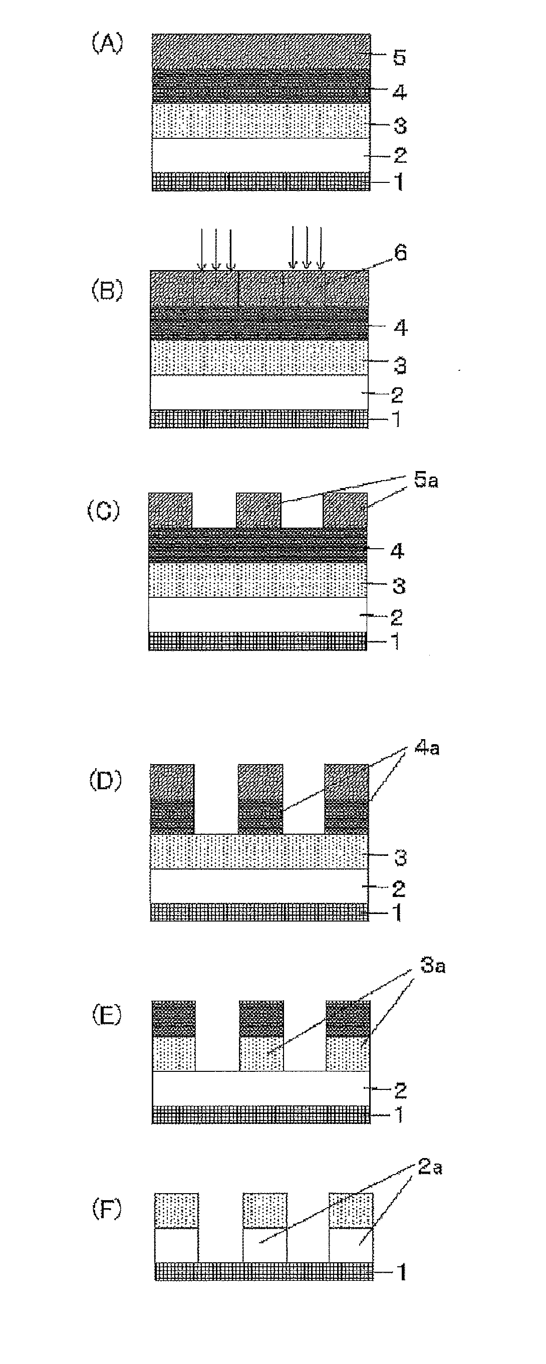
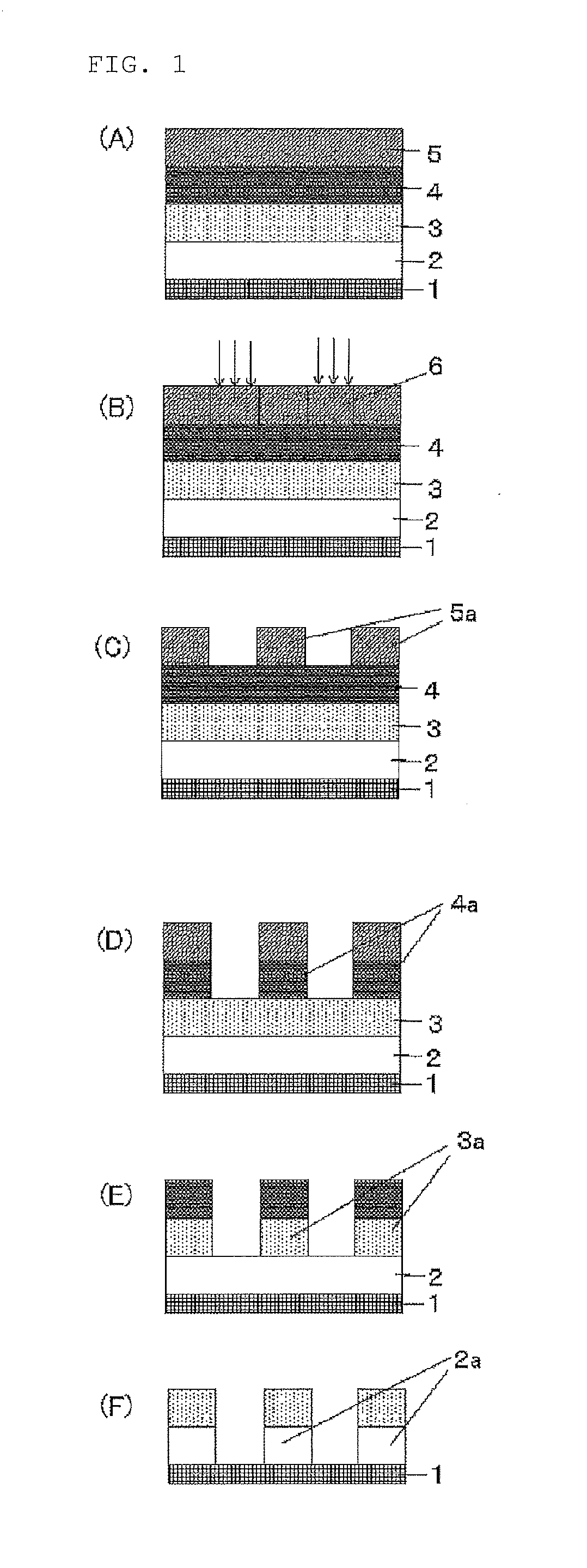
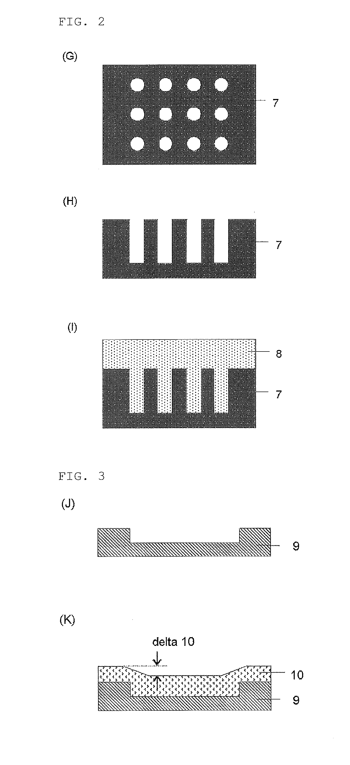
Organic film composition, process for forming organic film, patterning process, and compound
a composition and organic film technology, applied in the field of organic film composition, can solve the problems of resist compositions having a high resolution that tend to have a rather low etching resistance, the pattern cannot be precisely transferred to the substrate, and the pattern collapse phenomenon, etc., to achieve high filling/planarizing characteristics, and high dry etching resistance
- Summary
- Abstract
- Description
- Claims
- Application Information
AI Technical Summary
Benefits of technology
Problems solved by technology
Method used
Image

Examples
synthesis example 1
Synthesis of Compound (A-1)
[0185]
[0186]Under a nitrogen atmosphere, 80.0 g of Epoxy compound (E-1), 94.1 g of Carboxylic acid compound (C-5), and 600 g of 2-methoxy-1-propanol were mixed to homogeneous solution at a temperature of 100° C. Then, 5.7 g of benzyltriethylammonium chloride was added and stirred at a temperature of 120° C. for 12 hours. After being cooled to room temperature, 1,500 g of methyl isobutyl ketone was added, and the organic layer was washed with 300 g of pure water for 5 times. The organic layer was dried under reduced pressure to give Compound (A-1).
[0187]The weight average molecular weight (Mw) and the degree of dispersion (Mw / Mn) were measured by GPC to give following results:
(A-1): Mw=750, Mw / Mn=1.05
synthesis examples 2 to 19
Syntheses of Compounds (A-2) to (A-19)
[0188]Compounds (A-2) to (A-19) shown in Tables 2 to 4 were obtained as products in the same condition as in Synthesis Example 1 except that the epoxy compounds and the carboxylic acid compounds shown in Table 1 were used. The weight average molecular weights (Mw) and the degrees of dispersion (Mw / Mn) of these compounds were measured and shown in Tables 2 to 4.
TABLE 1CarboxylicCarboxylicCarboxylicEpoxyacidacidacidSynthesiscompoundcompoundcompoundcompoundExample(1)(1)(2)(3)1(E-1)(C-5)——80.0 g94.1 g2(E-2)(C-4)(C-6)—53.0 g55.6 g47.0 g3(E-3)(C-7)—— 75 g50.6 g4(E-4)(C-3)(C-6)—58.0 g17.3 g23.5 g5(E-4)(C-5)——58.0 g47.0 g6(E-5)(C-6)(C-7)—65.0 g23.5 g25.3 g7(E-6)(C-5)——51.0 g47.0 g8(E-6)(C-8)——51.0 g56.6 g9(E-6)(C-1)(C-6)—51.0 g17.8 g35.3 g10(E-6)(C-2)(C-5)—51.0 g14.2 g37.6 g11(E-7)(C-6)——40.5 g47.0 g12(E-7)(C-1)(C-5)—40.5 g17.8 g35.3 g13(E-7)(C-1)(C-2)(C-7)40.5 g7.1 g7.1 g40.4 g14(E-7)(C-1)(C-3)(C-7)40.5 g17.8 g8.6 g25.3 g15(E-8)(C-4)(C-6)—77.5 g27.8 g...
examples 1-1 to 1-24
, Comparative Examples 1-1 to 1-3
[0202]A silicon substrate is coated with each of the organic film compositions prepared above (UDL-1 to 24, Comparative UDL-1 to 3), baked under each condition shown in Table 6, and subsequently, the film thickness was measured. Then, a PGMEA solvent was dispensed thereon, allowed to stand for 30 seconds and spin dried, and baked at 100° C. for 60 seconds to evaporate the PGMEA. Subsequently, the film thickness was measured again to obtain a difference in the film thickness before and after the PGMEA treatment. On the formed organic films (resist under layer films), refractive indexes (n, k) at a wavelength of 193 nm were measured with an incident-angle variable spectroscopic ellipsometer (VASE) manufactured by J. A. Woollam Co., Inc. The results are shown in Table 6.
TABLE 6FilmFilmOpticalthicknessthicknesspropertyafter filmafter PGMEAb / a ×(193 nm)Organic filmformation:treatment:100Bakingnkcompositiona (Å)b (Å)(%)temperaturevaluevalueExample 1-1UDL-1...
PUM
| Property | Measurement | Unit |
|---|---|---|
| temperature | aaaaa | aaaaa |
| temperature | aaaaa | aaaaa |
| height | aaaaa | aaaaa |
Abstract
Description
Claims
Application Information