High-speed image sensor

a high-speed image sensor and sensor technology, applied in the field of high-speed imaging technology, can solve the problems of large spread of arrival time, inability to distinguish separately, and inability to reduce vertical mixing due to the different penetration depth and vertical diffusion due to the vertical component of random motion

Active Publication Date: 2020-08-20
ETOH TAKEHARU
View PDF0 Cites 4 Cited by
  • Summary
  • Abstract
  • Description
  • Claims
  • Application Information

AI Technical Summary

Benefits of technology

[0098]The roughness reduces an effective penetration depth of the incident light to the photoreceptive layer, which reduces the standard deviation of the arrival time of the signal charges from the photoreceptive area to the functional diffusion layer, and the temporal resolution.

Problems solved by technology

However, for (m2-m1)<2s, the peaks merge into one peak without a dip at the center and cannot be separately distinguished.
The distributed depth of the generation sites of signal electrons result in a large spread of the arrival time due to mixing of such signal electrons traveling different distances.
On the other hand, vertical mixing due to the different penetration depth and vertical diffusion due to the vertical component of the random motion cannot be reduced.
It is impossible to eliminate the effects of the distribution of the generation site and a vertical component of the random motion of a photoelectron on the spread of the arrival time.
Although a thinner photoreceptive layer reduces the time for the drift and the diffusion, it also reduces the sensitivity, since a large part of incident photons passes through the photoreceptive layer.
A third cause may be crosstalk due to light incident to the pixel boundary area.
Therefore, the crosstalk may be insignificant.
When the remaining photons horizontally spread in the relatively thick functional diffusion layer, false signal electrons generated in the collection devices to which the VH is not applied and cause crosstalk.
Since only a portion of the remaining photons causes the crosstalk, the effect on the captured images becomes practically insignificant.

Method used


Image

  • High-speed image sensor
  • High-speed image sensor
  • High-speed image sensor

Examples


first embodiment

1. First Embodiment

[0117]FIG. 7 shows a cross section 29 of a pixel of an image sensor according to a first embodiment of the invention. The image sensor includes three stacked layers: a light collection layer 30, an imaging layer 31, and a driver layer 32. The planar view is shown in FIG. 2.

[0118]The imaging layer and the driver layer are electrically connected through a bump layer 33. The light collection layer 30 includes a micro lens 34 and a light guide 35.

[0119]The imaging layer comprises a first light shield layer 36 (0.3 micrometers), a first insulation layer 37 (0.1 micrometers), a photoreceptive layer 38 made with a low-concentration n-type silicon layer (7 micrometers), a second light shield layer 39 (0.3 micrometers), a second insulation layer 40 (0.1 micron), a functional diffusion layer 41 (3 micrometers), a third insulation layer 42 (0.01 micrometers), and a metal circuit layer 43 (7 micrometers). The values in parentheses indicate the thicknesses of the layers. The l...

second embodiment

2. Second Embodiment

[0127]FIG. 8 shows a cross section 46 of a pixel in a second embodiment of the invention. The structure according to the embodiment includes a p-well 2, having no second light shield and no second insulation layer.

[0128]Hereafter, the first and the second embodiments are explained, assuming that the signal charge is an electron. The first and second embodiments achieve similar functions.

[0129]A high voltage applied to an electrode of one of the charge collection devices is VH=0 V and a low voltage applied to the electrodes of other charge collection devices is VL=−3 V.

[0130]Channels are formed on the bottom surface of the functional diffusion layer and above the electrodes of the charge collection devices.

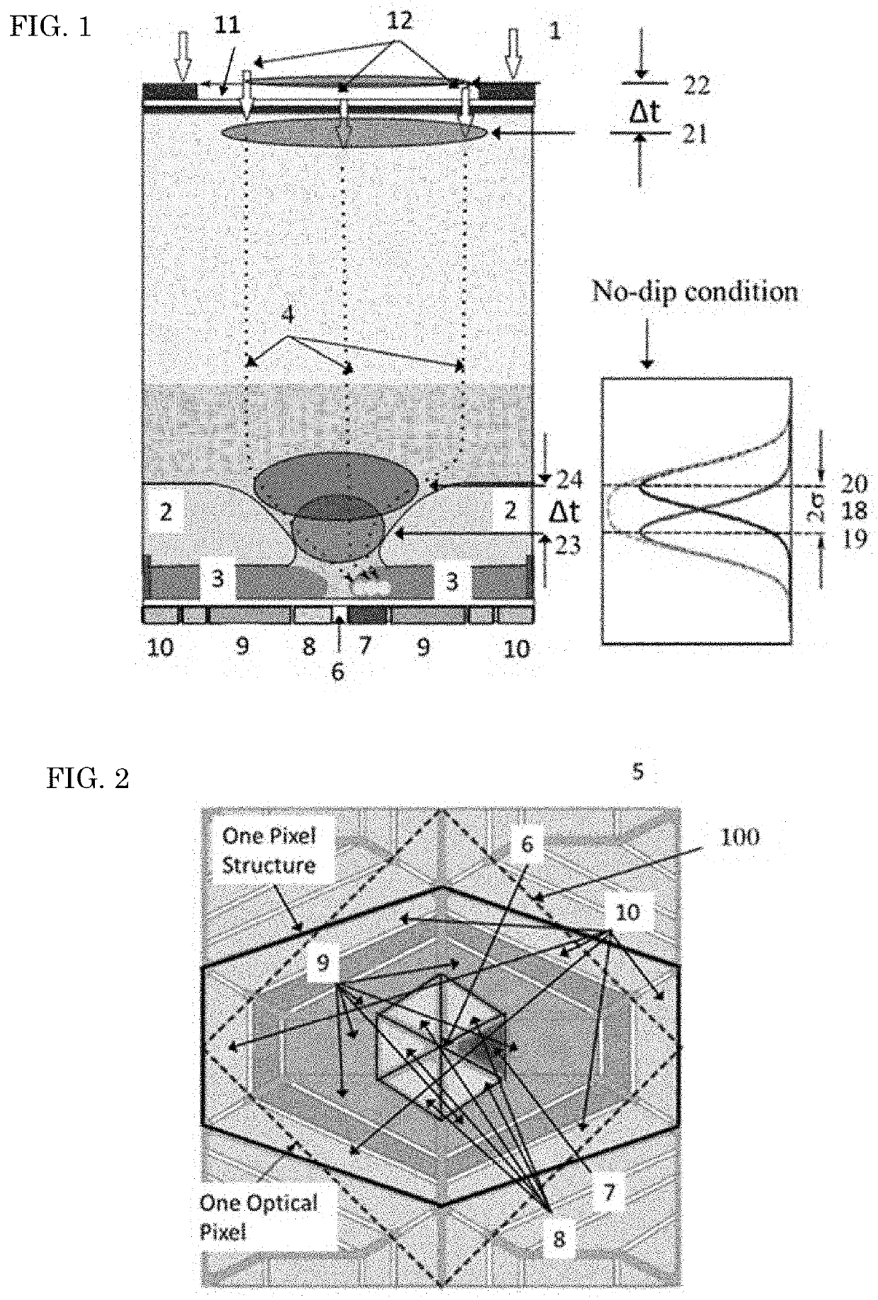
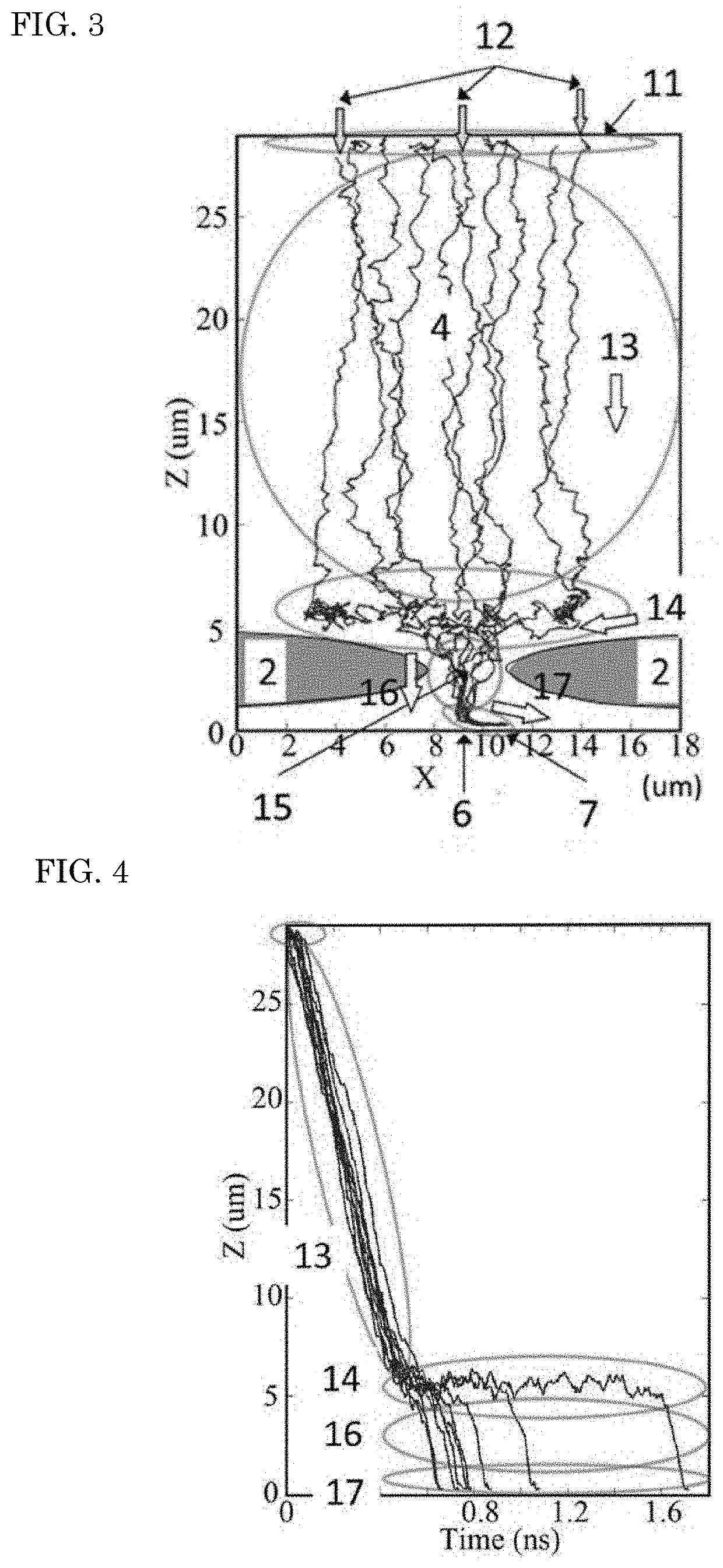
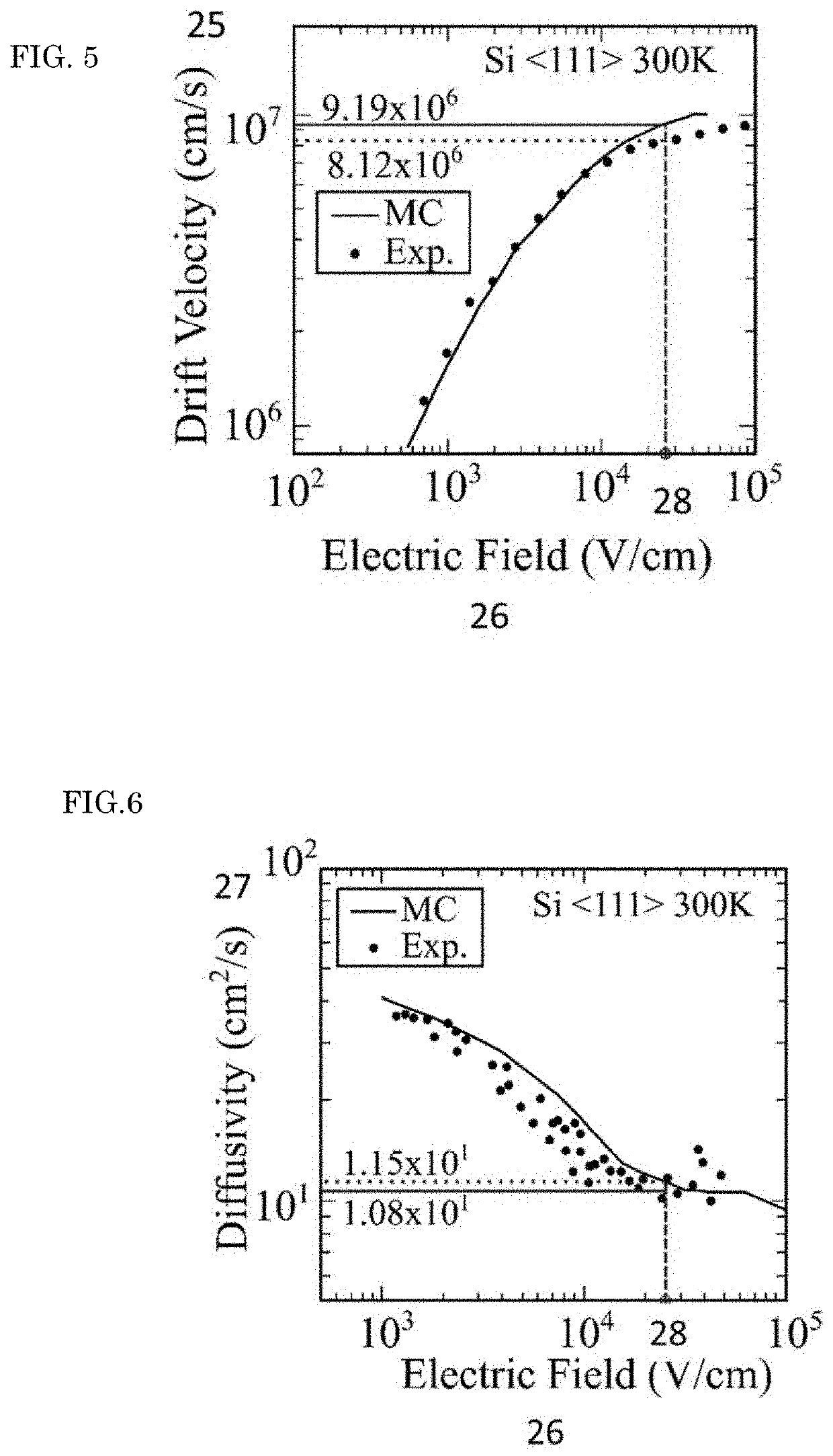
[0131]A backside voltage applied to the silicon layer (photoreceptive layer) inside the DTI is −20 V, which makes the vertical field in the photoreceptive layer equal to a critical field 28 (=25 kV / cm) as shown in FIG. 10.

[0132]Incident light is focused by a mic...

third embodiment

3. Third Embodiment

[0152]FIG. 12 shows a cross section 50 of a pixel according to a third embodiment of the invention.

[0153]A light collection layer 53 includes an on-chip Fresnel lens made with silicon oxide 51 and a light guide with silicon nitride 52.

[0154]The structure according to the embodiment also includes a funnel-shaped p-well 54 instead of the DTI. To suppress crosstalk due to spreading incident light, the photoreceptive layer is 30-micrometer thick, which absorbs 99.9% of incident light and leaves only 0.1% reaching the front side even for light of 700 nanometers. However, the thickness results in a slightly long temporal resolution.

[0155]A p-well of this special shape is formed as follows: a 3-micrometer thick intrinsic or low-concentration silicon layer is formed through epitaxial growth; boron ions are implanted with a mask with a frame-like opening around the pixel border; the process is repeated while the mask area is being decreased, and; finally, a thermal diffusi...


PUM


Abstract

A backside-illuminated multi-collection-gate image sensor is expected to achieve ultra-high-speed imaging. Signal electrons generated by incident light are collected to the pixel center of the front side and distributed to multiple collection gates placed around the center at a very short time interval. The temporal resolution is measured by the spread of arrival times of signal electrons to a collection gate. The major cause of the spread is mixing of signal electrons generated near the pixel border travelling a longer horizontal distance to the pixel center and those generated near the pixel center. Suppression of the horizontal travel time effectively decreases the standard deviation of the distribution of the arrival time. Therefore, devices to suppress the effects of the horizontal motion are introduced, such as a pipe-like photoelectron conversion layer with a much narrower cross section than the pixel area and a funnel-like photoelectron conversion layer.

Description

FIELD OF THE INVENTION[0001]The present invention relates to high-speed imaging technology.[0002]An existing silicon image sensor can capture consecutive images in one shot at the frame interval of about 10 nanoseconds (ns). Faster imaging with a frame interval down to 100 pico-seconds (ps), which is 1 / 100 of the shortest frame interval of the existing image sensors, is enabled by the invention. Image sensors with this such short temporal resolution may be used in scientific and industrial measurement apparatuses based on lifetime measurements, such as fluorescence lifetime imaging microscopy (FLIM) for observation of activities in cells, and time-of-flight (TOF) measurements, such as a 3-dimensional light detection and ranging sensor (LIDAR).BACKGROUND OF THE INVENTION1. Structure and Function of Backside-Illuminated Multi-Collection-Gate Image Sensors[0003]A Backside-Illuminated Multi-Collection-Gate image sensor (BSI MCG image sensor) including an array of pixels for ultra-highsp...

Claims


Application Information

Patent Timeline
Patent Type & Authority Applications(United States)
IPC IPC(8): H01L27/146H01L27/148H04N5/378
CPCH01L27/1464H01L27/14818H04N5/378H01L27/14605H01L27/144H01L27/146H01L27/148G01S7/4816G01S17/89H01L27/14607H01L27/1461H01L27/14627H01L27/14629H04N25/70H04N25/75
Inventor ETOH, TAKEHARU
Owner ETOH TAKEHARU
Why Eureka
Try Eureka