Indium nitride nanopillar epitaxial wafer grown on aluminum foil substrate and preparation method of indium nitride nanopillar epitaxial wafer

Active Publication Date: 2020-10-29
SOUTH CHINA UNIV OF TECH
View PDF2 Cites 2 Cited by
  • Summary
  • Abstract
  • Description
  • Claims
  • Application Information

AI Technical Summary

Benefits of technology

The present invention aims to provide an InN nanorod epitaxial wafer grown on an aluminum foil substrate. By banning the aluminum oxide amorphous layer with high-activity nitrogen plasma, the nucleation sites of AlN are formed, which facilitate the growth of InN nanorods with a uniform diameter. This solves the technical problem of providing an upright InN nanorod with a uniform diameter on an aluminum foil substrate by epitaxial growth. The defect density of the InN nanorod epitaxial layer is greatly reduced, the radiation recombination efficiency of current carriers is improved, and the luminous efficiency of nitride devices such as a semiconductor laser or an LED is significantly increased. The present invention also provides a method for preparing thisInN nanorod epitaxial wafer, which has the advantages of a simple growth process, controllable appearance of the nanorod, and low preparation cost.

Problems solved by technology

However, due to the low thermal conductivity (45W / m·K) of sapphire, a high-power nitride semiconductor device using sapphire as a substrate cannot efficiently dissipate heat, and the heat may be accumulated to increase the temperature and deteriorate the nitride semiconductor device, resulting in poor device performance and short lifetime.
Due to the distinct lattice mismatch and thermal mismatch between Si and InN and the different distribution ratio of In and N atoms on the substrate surface in the initial growth stage, the grown InN nanorods may have uneven height, diameter and length, poor orderliness, etc.
In addition, when preparing a nitride light-emitting device by growing InN nanorods epitaxially on a Si substrate, due to the light absorption feature of the Si substrate, the light-emitting efficiency of the prepared device is low, and therefore the Si substrate should be removed when preparing the device, which complicates the preparation of the device.
Therefore, the nanorods cannot nucleate and grow on the surface of the substrate through a conventional growth method such as MOCVD (metal organic chemical vapor deposition), CVD (chemical vapor deposition) and PLD (pulsed laser deposition), and nanorods with uniform diameter, high orderliness and vertical growth cannot be epitaxially grown.

Method used


Image

  • Indium nitride nanopillar epitaxial wafer grown on aluminum foil substrate and preparation method of indium nitride nanopillar epitaxial wafer

Examples


example 1

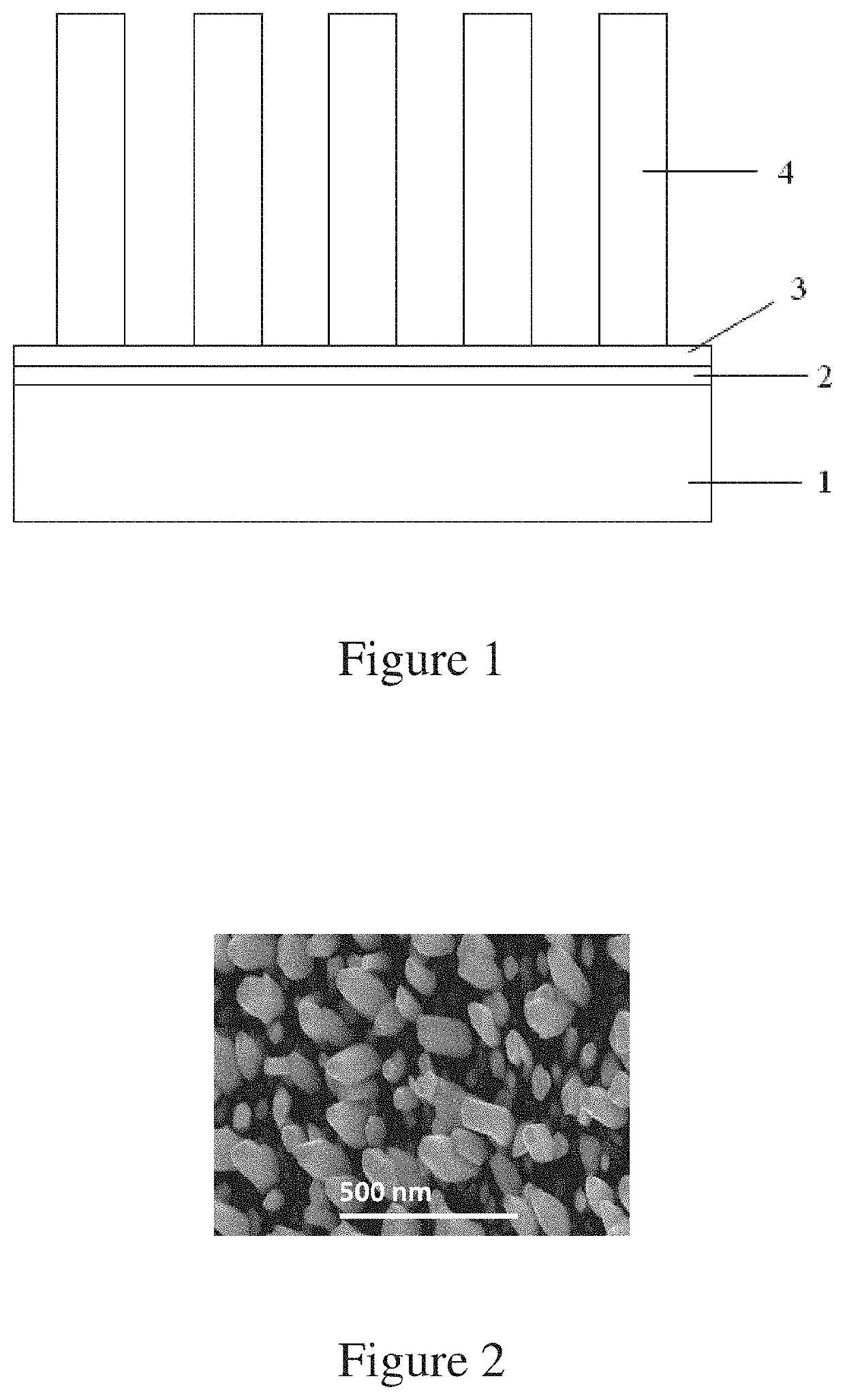
[0038]An InN nanorod epitaxial wafer grown on an aluminum foil substrate of this Example sequentially comprises, from bottom to top, an aluminum foil substrate, an amorphous aluminum oxide layer, an AlN layer, and an InN nanorod layer.

[0039]The preparation method of the InN nanorod epitaxial wafer grown on the aluminum foil substrate in the Example comprises:

[0040](1) Selection of a substrate: selecting a commonly used commercial aluminum foil substrate (with an oxidized surface);

[0041](2) polishing and cleaning the substrate: mechanically polishing and grinding the aluminum foil to obtain a flat surface; then placing the aluminum foil with the flat surface into absolute ethyl alcohol for ultrasonic treatment for 1 min to remove organic pollutants and sticky particles, then placing the aluminum foil into deionized water for ultrasonic treatment for 1 min to remove surface impurities, and drying same by high-purity dry nitrogen gas;

[0042](3) in-situ annealing to further remove contam...

example 2

[0047]An InN nanorod epitaxial wafer grown on an aluminum foil substrate of this Example sequentially comprises, from bottom to top, an aluminum foil substrate, an amorphous aluminum oxide layer, an AlN layer, and an InN nanorod layer. The InN nanorod layer 4 adopts AlN as nucleation sites, and nucleating on the AlN to grow InN nanorods.

[0048]The preparation method of the InN nanorod epitaxial wafer grown on the aluminum foil substrate in the Example comprises:

[0049](1) Selection of a substrate and the crystal orientation thereof: selecting a commonly used commercial aluminum foil substrate;

[0050](2) polishing and cleaning the substrate: mechanically polishing and grinding the aluminum foil to obtain a flat surface; then placing the aluminum foil with the flat surface into absolute ethyl alcohol for ultrasonic treatment for 2 min to remove organic pollutants and sticky particles, then placing the aluminum foil into deionized water for ultrasonic treatment for 2 min to remove surface...


PUM


Abstract

An InN nanorod epitaxial wafer grown on an aluminum foil substrate (1) sequentially comprises the aluminum foil substrate (1), an amorphous aluminum oxide layer (2), an AlN layer (3) and an InN nanorod layer, (4) from bottom to top. The wafer can be prepared by pretreating the aluminum foil substrate with an oxidized surface and carrying out an in-situ annealing treatment; then, in a molecular beam epitaxial growth process, forming AlN nucleation sites on the annealed aluminum foil substrate, nucleating on the AlN and growing InN nanorods on the AlN. where the substrate temperature is 400-700° C., the pressure of a reaction chamber is 4.0-10.0×10⁻⁵ Torr and the beam ratio of V / III is 20-40.

Description

TECHNICAL FIELD[0001]The invention belongs to the technical field of nitride semiconductor devices, and relates to an indium nitride (InN) nanorod epitaxial wafer and a preparation method thereof, in particular to an InN nanorod epitaxial wafer grown on an aluminum foil substrate and a preparation method thereof.BACKGROUND ART[0002]Group III-V nitrides are widely used in Light Emitting Diodes (LEDs), lasers, and optoelectronic devices due to their advantages of stable physicochemical properties, high thermal conductivity, and high electron saturation velocity. Among group III-V nitrides, indium nitride (InN) is of increasing interest to researchers due to its unique advantages. In group III nitride semiconductors, InN has the smallest effective electron mass, the highest carrier mobility, and the highest saturation transition velocity, which are extremely advantageous for developing high-speed electronic devices. Moreover, InN has the smallest direct band gap with a forbidden band w...

Claims


Application Information

Patent Timeline
IPC IPC(8): H01L29/20H01L29/06H01L21/02
CPCH01L29/2003H01L29/0676H01L21/02488H01L21/02603H01L21/02425H01L21/0254H01L33/32H01L21/02458H01L21/02472H01L21/02502H01L21/02631H01L21/02658B82Y30/00B82Y40/00H01L21/02645Y02P70/50
Inventor LI, GUOQIANGGAO, FANGLIANGXU, ZHENZHU
Owner SOUTH CHINA UNIV OF TECH
Why Eureka
Try Eureka