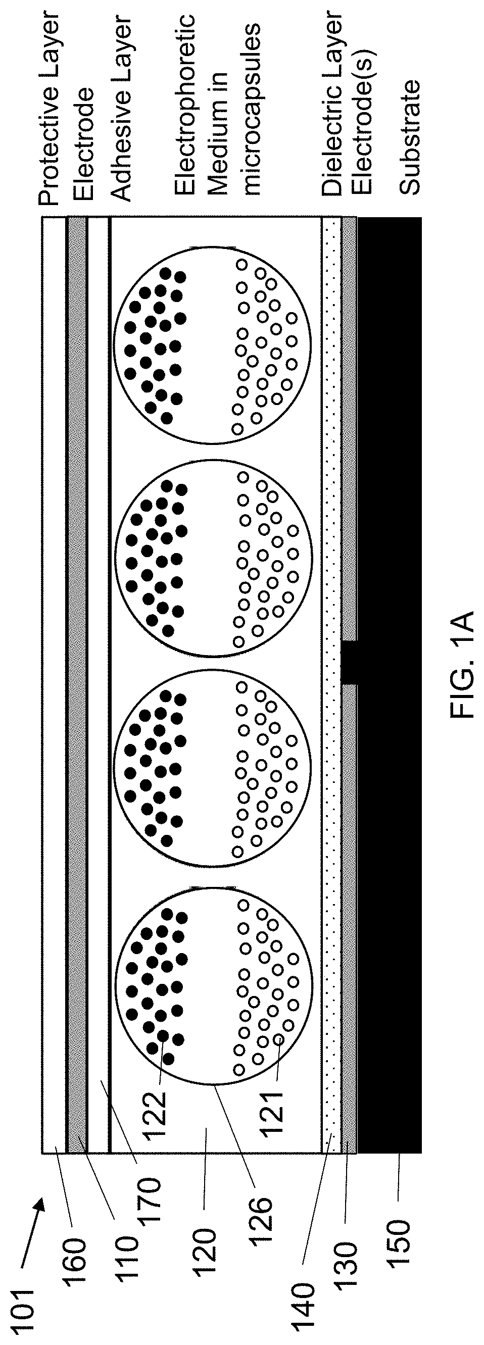
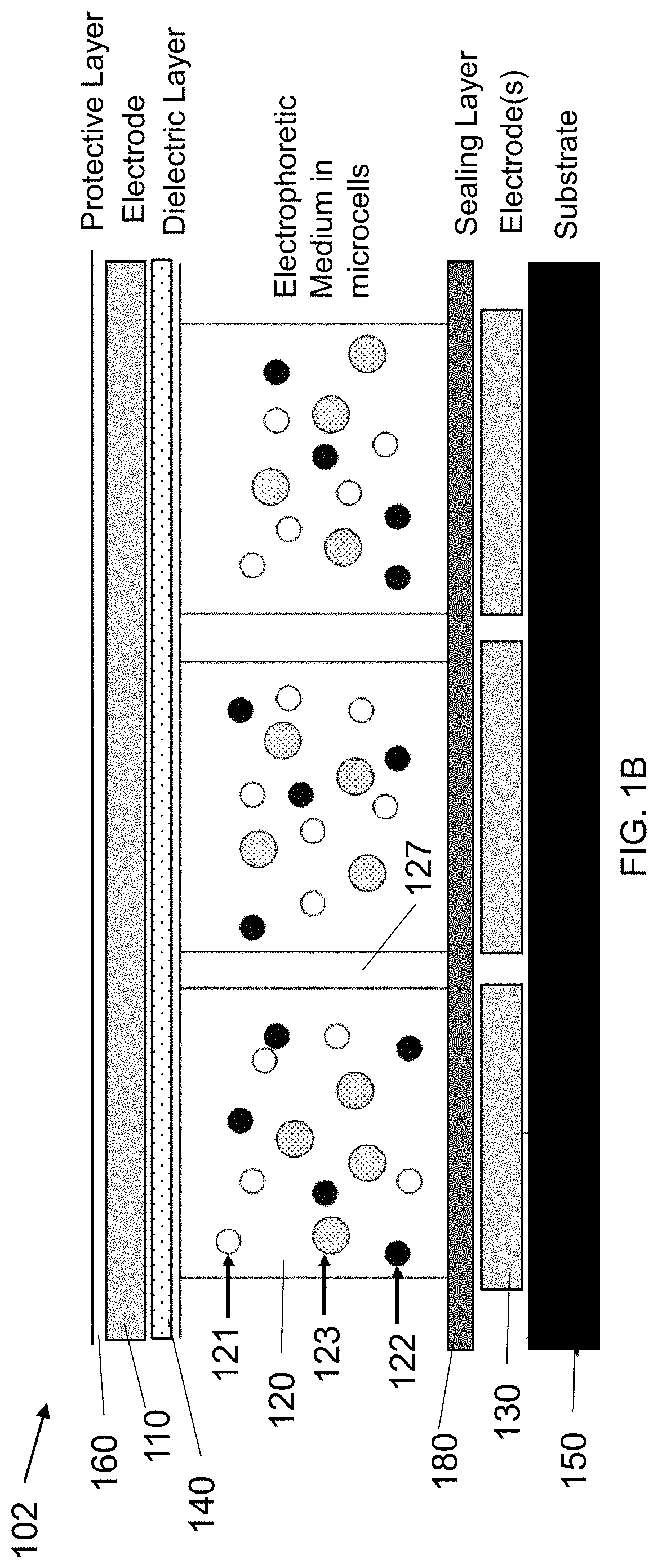
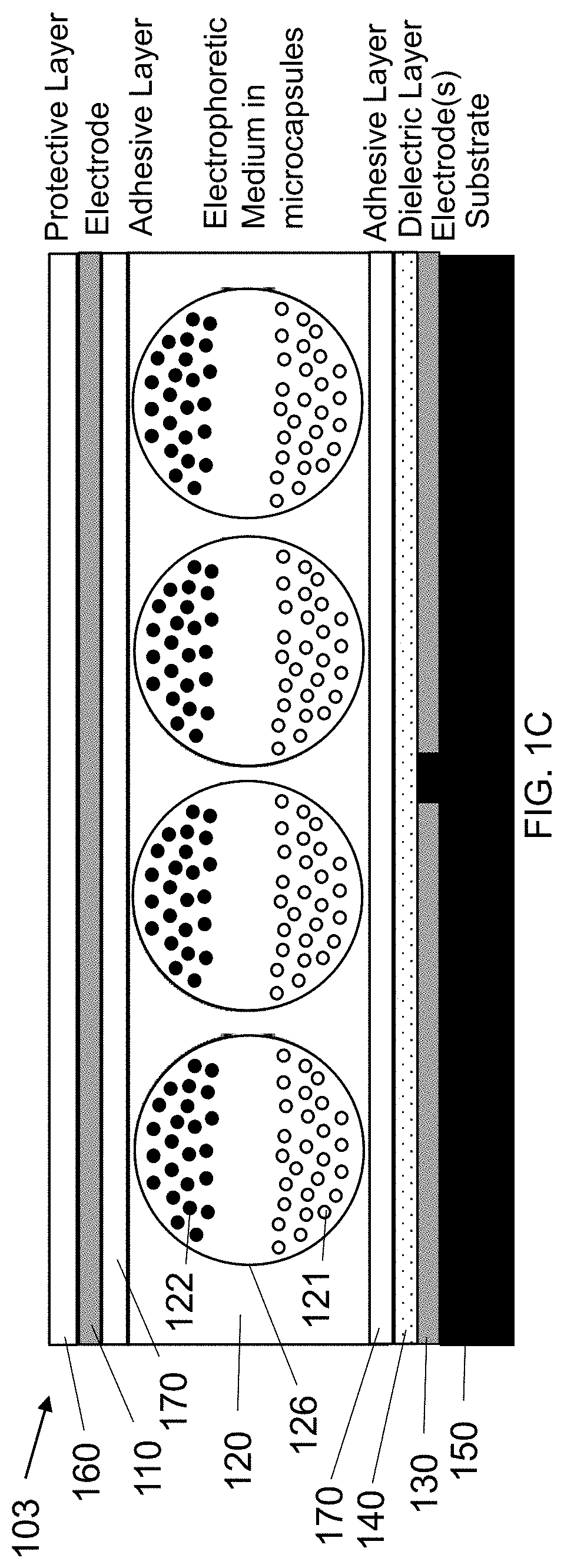
Layered structure with high dielectric constant for use with active matrix backplanes
- Summary
- Abstract
- Description
- Claims
- Application Information
AI Technical Summary
Benefits of technology
Problems solved by technology
Method used
Image

Examples
example 2
Color Gamut Due to Dielectric Layer
[0068]As illustrated in the model circuits, the addition of the capacitance C5 to the dielectric layer slightly changes the voltages within the imaging layers of the display, and might be expected to affect the number of colors that can be achieved. The amount of color lost due to this voltage drop was experimentally verified using a four pigment (CMYW) test cell including silicon nitride layers of different thickness over the rear electrode of the display. Details of the test cell can be found in U.S. Pat. No. 9,921,451, which is incorporated by reference herein in its entirety. The results are shown below in Table 1.
TABLE 1Effect of silicon nitride dielectric on color gamut of four-particle (CMYW) electrophoretic medium in a test cell.Silicon nitrideCapacitanceColor gamutthickness (nm)estimated (nF / cm2)measured (dE3)0n / a2100020332180005013313000758911000
[0069]Table 1 shows the estimated capacitance of the dielectric based upon measured thickness,...
example 3
in Electrochemical Degradation in Electrophoretic Test Cells
[0072]In addition to improving the response of the electrophoretic medium (above), the effect of an added dielectric layer on longevity of a test display was also evaluated. Two test displays of approximately 8″ diagonal were prepared using the CMYW four particle electrophoretic medium of Example 2. The control used a standard active matrix TFT backplane, as found in a commercial eReader. In the other test display, the pixel electrodes were coated with 30 nm of tantalum oxide. The continuity of the tantalum oxide layer was not perfect, as shown in the graph of FIG. 12. If the tantalum oxide was without pinholes or defects, it would be expected that there would be considerably less resistive current density for the tantalum oxide “blocked” backplane. The displays were driven in a highly DC-imbalanced way using a sequence of (a) 30V for 3 seconds, followed by (b) grounding for 20 ms, then (c) floating for 6 seconds. This test...
PUM
| Property | Measurement | Unit |
|---|---|---|
| Thickness | aaaaa | aaaaa |
| Thickness | aaaaa | aaaaa |
| Thickness | aaaaa | aaaaa |
Abstract
Description
Claims
Application Information