Silicon carbide structure, device, and method

a technology of silicon carbide and mems, which is applied in the direction of microstructural devices, microstructures, coatings, etc., can solve the problems of high surface roughness, high residual stress of 3c-sic material layers grown on silicon substrates, and high dislocation density, so as to facilitate the formation of movable suspended material structures, high thermal conductivity, and high thermal conductivity

Active Publication Date: 2020-12-31
THE UNITED STATES OF AMERICA AS REPRESENTED BY THE SECRETARY OF THE NAVY
View PDF0 Cites 2 Cited by
  • Summary
  • Abstract
  • Description
  • Claims
  • Application Information

AI Technical Summary

Benefits of technology

[0005]The present invention provides a structure and method of making a suspended beam silicon carbide MEMS structure (e.g., gyroscope, accelerometer, oscillator, inertial sensor) with low capacitance and good thermal expansion match of the suspended beam SiC material and anchor material to the first substrate SiC material. SiC provides higher modulus, higher density, and higher thermal conductivity than silicon, which are desirable properties for SiC MEMS systems. Hexagonal SiC provides superior isoelasticity (rotation symmetry) versus silicon reducing errors in gyroscope functioning. SiC provides higher stiffness and fracture toughness than silicon, improving shock resistance for high-G applications (e.g., missiles, rail gun projectile). SiC provides improved radiation hardness compared to silicon. SiC single-crystal hexagonal material bonded to SiC single-crystal hexagonal first substrate provides good thermal expansion match.
[0006]SiC material properties provide significant advantages for MEMS devices. A thick top hexagonal SiC N+ suspended beam enables lower noise. The use of single-crystal hexagonal SiC for both the top N+ suspended beams, the anchor material structure, and the optional electrostatic sense electrode and the bottom handle first substrate enables good thermal expansion match and low stresses. The use of semi-insulating SiC bottom first substrate enables low parasitic capacitance for electrostatic sense electrode and thus improved noise properties. Several other features (e.g., top side ohmic contact, bottom side ohmic contact, undercut, recesses) are described to implement improved SiC MEMS structures. SiC material has higher modulus, higher density, higher thermal conductivity, improved rotational symmetry, higher fracture strength, higher shock resistance, high radiation resistance than silicon.

Problems solved by technology

3C-SiC material layers grown on silicon substrate typically have high residual stress, high dislocation density, and high surface roughness.
There is significant thermal expansion mismatch between the 3C-SiC epitaxial layer and a silicon substrate.

Method used


Image

  • Silicon carbide structure, device, and method
  • Silicon carbide structure, device, and method
  • Silicon carbide structure, device, and method

Examples


example device embodiment 1

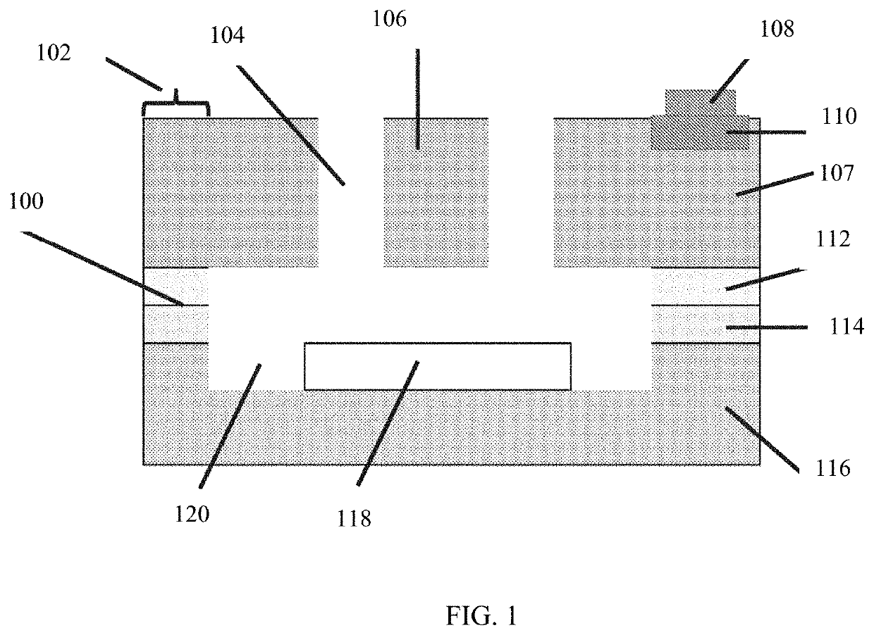
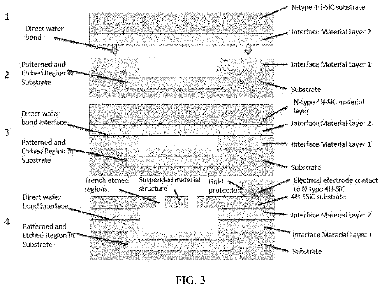
[0074]In one embodiment, one or more than one suspended material structures comprise a hexagonal single-crystal SiC material having a first surface and a second surface with each suspended material structure attached (fixed) to one or more than one anchor material structures that are bonded to a substrate with no interface material layer, one optional interface material layer or more than one optional interface material layers at the interface between the hexagonal single-crystal SiC material layer and the substrate. The anchor material structure comprises hexagonal single-crystal hexagonal SiC material. The anchor material structure and the suspended material structure are formed from a single-crystal hexagonal SiC material and the anchor material structure is bonded (attached) to the substrate and the suspended material structure is not attached to the substrate. The substrate may be a hexagonal single-crystal SiC substrate which may be conductive with N-type doping, conductive wi...

example device embodiment 2

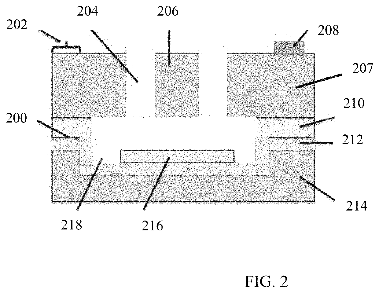
[0120]In another embodiment, this invention provides one or more than one suspended material structure(s) that comprise hexagonal single-crystal SiC material having a first surface and a second surface with each suspended material structure attached (fixed) to one or more than one anchor material structures that are bonded to a first substrate with no interface material layer, one optional interface material layer or more than one optional interface material layers at the interface between the hexagonal single-crystal SiC material layer and the first substrate. The anchor material structure comprise hexagonal single-crystal hexagonal SiC material. The anchor material structure and the suspended material structure may be formed from a single-crystal hexagonal SiC material and the anchor material structure is bonded (attached) to the first substrate and the suspended material structure is not attached to the first substrate. The substrate may be a single crystal SiC substrate.

[0121]Th...


PUM

PropertyMeasurementUnit
thicknessaaaaaaaaaa
thicknessaaaaaaaaaa
thicknessaaaaaaaaaa

Abstract

A method of fabricating suspended beam silicon carbide microelectromechanical (MEMS) structure with low capacitance and good thermal expansion match. A suspended material structure is attached to an anchor material structure that is direct wafer bonded to a substrate. The anchor material structure and the suspended material structure are formed from either a hexagonal single-crystal SiC material, and the anchor material structure is bonded to the substrate while the suspended material structure does not have to be attached to the substrate. The substrate may be a semi-insulating or insulating SiC substrate. The substrate may have an etched recess region on the substrate first surface to facilitate the formation of the movable suspended material structures. The substrate may have patterned electrical electrodes on the substrate first surface, within recesses etched into the substrate.

Description

PRIORITY CLAIM[0001]The present application is a divisional application of U.S. application Ser. No. 15 / 908,682 filed on Feb. 28, 2018 by Francis J. Kub et al., entitled “SILICON CARBIDE STRUCTURE, DEVICE, AND METHOD, which claimed the benefit of U.S. Provisional Application No. 62 / 464,814 filed on Feb. 28, 2017 by Francis J. Kub et al., entitled “SILICON CARBIDE STRUCTURE, DEVICE, AND METHOD,” the entire contents of both are incorporated herein by reference.BACKGROUND OF THE INVENTIONField of the Invention[0002]The present invention relates to a structure and method of fabricating thick beam silicon carbide MEMS structure with low capacitance and good thermal expansion match.Description of the Prior Art[0003]3C-SiC is often used for microelectromechanical (MEMS) device structures. 3C-SiC material layers grown on silicon substrate typically have high residual stress, high dislocation density, and high surface roughness. The 3C-SiC material layers grown on a silicon substrate can be ...

Claims


Application Information

Patent Timeline
Patent Type & Authority Applications(United States)
IPC IPC(8): B81B3/00B81C1/00H01L29/16
CPCB81B2201/0235B81B2203/0118B81B2203/0109B81C1/00531B81B3/0072B81C2201/019B81B2201/0242H01L29/1608B81B3/0021B81B2203/0127
Inventor KUB, FRANCIS J.HOBART, KARL D.IMHOFF, EUGENE A.MYERS-WARD, RACHAEL L.
Owner THE UNITED STATES OF AMERICA AS REPRESENTED BY THE SECRETARY OF THE NAVY
Why Eureka
Try Eureka