Two-Dimensional Material Detector Based on Asymmetrically Integrated Optical Microstrip Antenna

a technology of optical microstrips and detectors, applied in the direction of resonant antennas, substantially flat resonant elements, basic electric elements, etc., can solve the problems of no generally reliable two-dimensional material doping methods, large influence of two-dimensional heterojunction, and inability to provide power supply for each piece of equipment, etc., to achieve high process compatibility, achieve easy operation, and reduce the effect of manufacturing process

Pending Publication Date: 2022-03-17
SHANGHAI INST OF TECHNICAL PHYSICS - CHINESE ACAD OF SCI
View PDF0 Cites 2 Cited by
  • Summary
  • Abstract
  • Description
  • Claims
  • Application Information

AI Technical Summary

Benefits of technology

[0015]3. The optical structure of the detector and the active material are integrated on the substrate, which can be achieved easily due to high

Problems solved by technology

Unfortunately, photodetectors must meet certain requirements to be specifically used in related industries and researches.
It is impractical to provide a power supply for each piece of equipment in many applications such as outdoor environmental monitoring and wearable medical monitoring based on wireless sensor networks.
Since so far there is no generally reliable doping method for two-dimensional materials.
The problem of the former is that a two-dimensional heterojunction may be greatly affected by the different band structures of the heterogeneous materials and especially affected by the interface.
Thus, it is difficult to effectively control the transport prop

Method used


Image

  • Two-Dimensional Material Detector Based on Asymmetrically Integrated Optical Microstrip Antenna
  • Two-Dimensional Material Detector Based on Asymmetrically Integrated Optical Microstrip Antenna

Examples


example

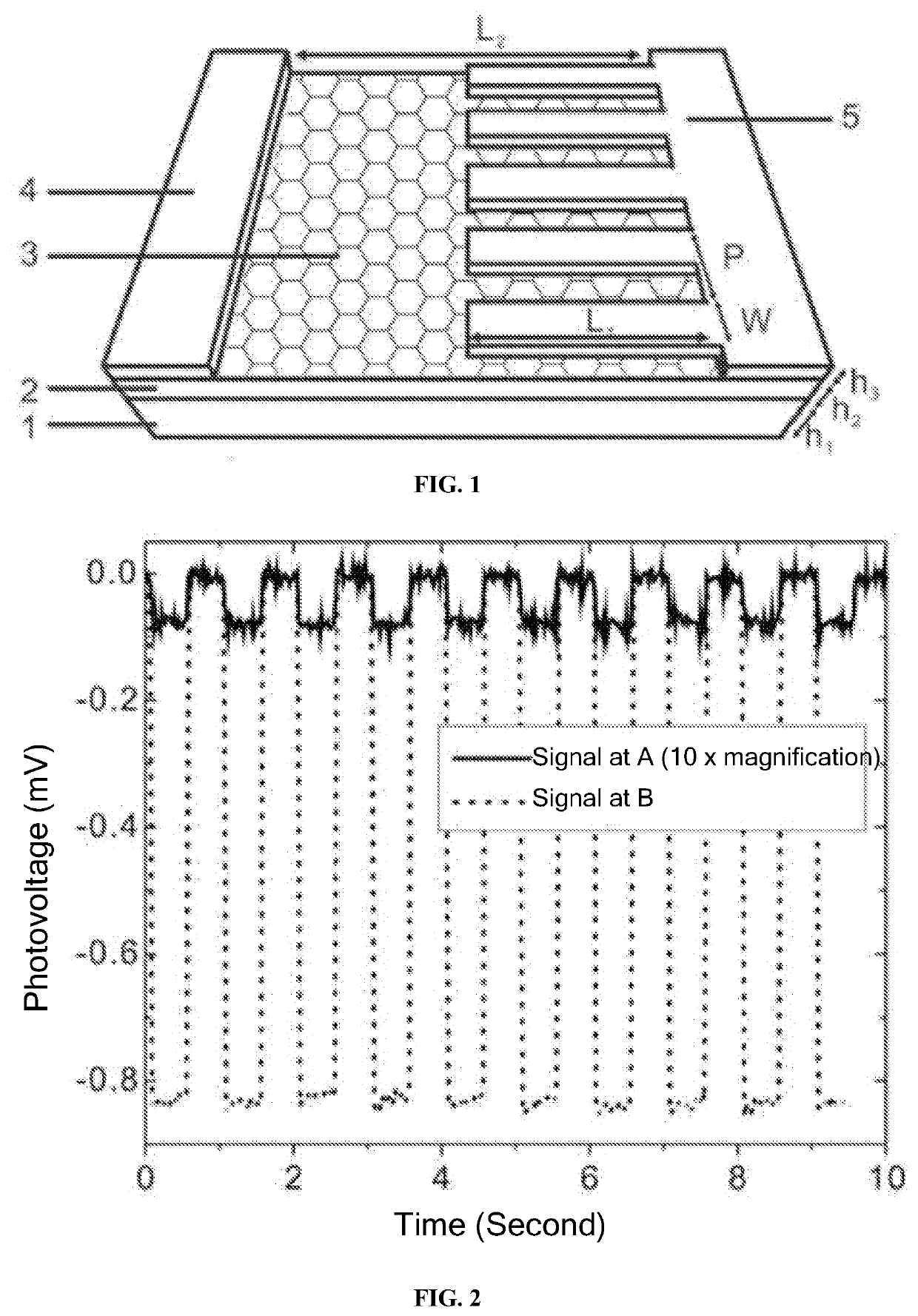
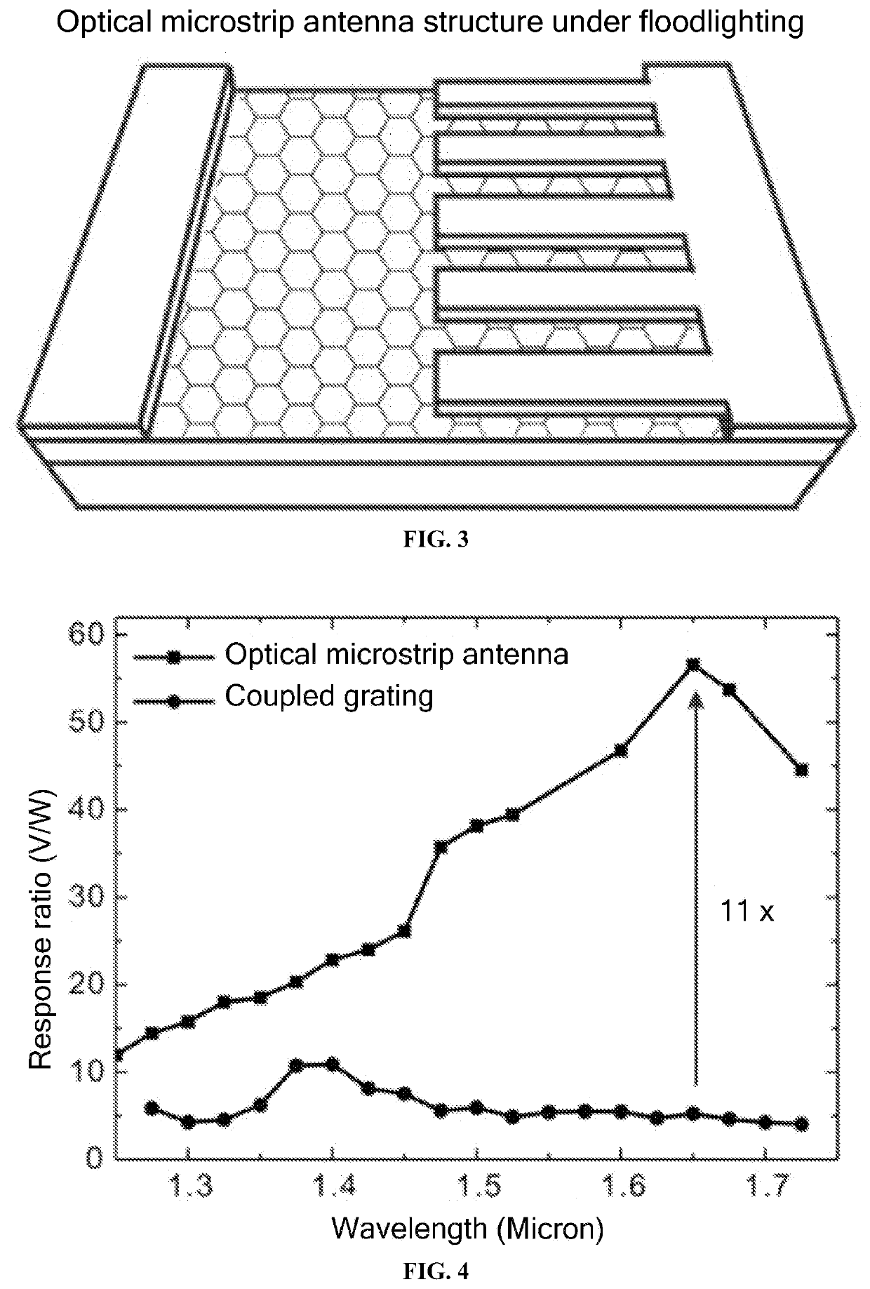
[0027]The graphene detector with asymmetrically integrated optical microstrip antennas in this example works at a wavelength of 1.65 μm. An optimized periodic unit was designed with the following structural dimensions: P=590 nm, W=283 nm, L1=5 μm, L2=10 μm, h1=110 nm, h2=30 nm, and h3=45 nm. The metal reflecting layer (1) was formed by Cr (20 nm) / Au (90 nm). The dielectric spacer layer (2) was an aluminum sesquioxide dielectric layer that was transparent to the working waveband. The thickness of layer (2) is specifically designed according to the requirement of the optical microstrip antenna. The two-dimensional active material (3) was a single layer of graphene grown by copper-based CVD and transferred by a wet chemistry method. The source electrode (4) and the drain electrode (5) integrated with the metal strip array were made of Cr (5 nm) / Au (45 nm). As a reference control, a common graphene device was asymmetrically integrated with a light-coupling grating with the same structur...


PUM


Abstract

The present disclosure provides a two-dimensional material detector with an asymmetrically integrated optical microstrip antenna, structurally including a metal reflecting surface, a dielectric spacer layer, a two-dimensional active material layer, a top source electrode, and a drain electrode integrated with a metal strip array. Self-driven photoresponse of a metal/two-dimensional material/metal structure is induced by a Schottky junction formed due to contact between the two-dimensional material and the metal. The asymmetrically integrated optical microstrip antennas break the symmetry between the two contact/two-dimensional material junctions. Light absorption in the contact/two-dimensional material junction integrated with optical patch antennas is significantly enhanced by efficient light in-coupling and intensified light localization; meanwhile, the extended boundary of the contact/two-dimensional material junction enlarges the photocurrent collection area. The light absorption in the other contact/two-dimensional material junction is significantly inhibited by a metal bottom surface which is very close to the two-dimensional material.

Description

CROSS REFERENCE TO RELATED APPLICATION[0001]This application claims priority to Chinese Patent Application No. 202010965512.7, filed Sep. 15, 2020, which is herein incorporated by reference in its entirety.TECHNICAL FIELD[0002]The present disclosure relates to a two-dimensional material detector with asymmetrically integrated optical microstrip antennas, and in particular, to a two-dimensional material detector with asymmetrically integrated optical microstrip antennas allowing for self-driven photoresponse enhancement, and a design method thereof.BACKGROUND ART[0003]At present, photodetectors have been widely used in optical fiber communication, optical imaging, remote sensing, and biomedical analysis systems and have become an essential part in daily life. Unfortunately, photodetectors must meet certain requirements to be specifically used in related industries and researches. Due to different working waveband needs, it must be careful to select the energy band gap of a semiconduc...

Claims


Application Information

Patent Timeline
IPC IPC(8): H01L31/101H01Q9/04H01L31/0232
CPCH01L31/1013H01L31/02327H01Q9/0407H01L31/101H01Q1/2283H01L31/035209H01L31/112H01L31/0224
Inventor ZHOU, JINGGUO, SHANGKUNYU, YUJI, ZHAOYUDAI, XUDENG, JIECHEN, XIAOSHUANGCAI, QINGYUANCHU, ZESHILI, FANGZHELAN, MENGKE
Owner SHANGHAI INST OF TECHNICAL PHYSICS - CHINESE ACAD OF SCI
Why Eureka
Try Eureka