Method of making an improved field oxide isolation structure for semiconductor integrated circuits having higher field oxide threshold voltages

a technology of field oxide isolation and integrated circuit, which is applied in the direction of semiconductor devices, electrical apparatus, transistors, etc., can solve the problems of lateral oxidation of silicon substrates, reduced device feature sizes, and increased circuit density

Inactive Publication Date: 2000-04-25
TAIWAN SEMICON MFG CO LTD
View PDF8 Cites 7 Cited by
  • Summary
  • Abstract
  • Description
  • Claims
  • Application Information

AI Technical Summary

Benefits of technology

It is another object of this invention to provide these higher threshold voltages and reduced leakage currents by forming additional insulating sidewall portions along the perimeter of the field oxide regions which modify the channel-stop implant profile when the channel-stop implant dopant is implanted through the modified field oxide.
It is an object of this invention to provide a new structure and method for forming field oxide isolation regions by providing a modified LOCOS structure. The method consists of depositing a conformal insulating layer over the more conventional LOCOS field oxide, and anisotropically plasma etching back to form a thicker insulation over the perimeter of the LOCOS field oxide, commonly referred to as the "bird's beak". This modifies the profile of the channel-stop implant through the field oxide which provides a more robust isolation having increased field oxide threshold voltages (V.sub.th) and reduced leakage currents.
In summary, the method of forming the field isolation structure begins by providing a semiconductor substrate, such as a single-crystal silicon. A silicon oxide layer is formed on the surface of the silicon substrate to provide a stress-release pad oxide layer. A silicon nitride layer is deposited on the pad oxide layer, which provides an oxidation barrier layer. The silicon nitride layer and the pad oxide layer are patterned to leave portions over the device areas, while providing openings over the areas surrounding the device areas where the field oxide isolation regions are required. The silicon substrate is then thermally oxidized in the openings, while the silicon nitride layer prevents oxidation of the device areas, thereby forming a field oxide that by the LOCOS method results in thinner portions, commonly referred to as "bird's beak" on the perimeter of the field oxide extending under the silicon nitride layer. The silicon nitride and pad oxide layers are removed by wet etching exposing the device areas. A sacrificial oxide layer is formed by thermal oxidation in the device areas and is then removed by wet etching to remove any surface damage. Now, by the method of this invention, the shape of the LOCOS field oxide is modified by depositing a conformal insulating layer, such as silicon oxide (SiO.sub.2) deposited by chemical vapor deposition (CVD) on the substrate and over the LOCOS field oxide. The conformal insulating layer is anisotropically plasma etched back to the substrate leaving sidewall portions of the insulating layer on the thinner portions of the LOCOS field oxide, thereby modifying the shape of the field oxide by forming a thicker oxide layer over the bird's beak. As described later, this thicker oxide modifies the channel-stop implant profile, which increases the threshold voltages and / or reduces leakage currents, which eliminates the need for higher implant doses that are known to cause higher leakage currents. A thin oxide implant layer is formed on the device areas and a patterned photoresist implant mask is used to form P-wells by ion implantation, the channel-stop implant regions under the field oxide by implanting through the modified field oxide having the sidewall portions, and a deep implant to prevent latchup. The thicker field oxide at the perimeter resulting from the sidewall portions modifies the profile of the channel-stop implant in the substrate. This forms a channel-stop implant closer to the field oxide / substrate interface under the bird's beak, which results in increased threshold voltages and reduced leakage currents. Also, the thicker field oxide further increases the threshold voltage.

Problems solved by technology

However, the LOCOS methods even with implanting through the field oxide, has several problems as the device feature sizes decrease and the circuit density increases.
One problem is the lateral oxidation of the silicon substrate under the silicon nitride mask forming what are commonly referred to in the industry as "birds' beaks."
Also, as the width of the LOCOS between adjacent device areas decreases, the channel-stop implant through the field oxide becomes less effective, especially under the bird's beaks, and therefore requires a higher implant dose.
However, this results in higher leakage currents that shorten the refresh cycle time and reduce the DRAM performance.
Typically these methods require more complex processing than the more conventional LOCOS technique.
However, one problem that arises when narrow field oxide regions are formed by the more conventional LOCOS method is that the birds' beaks formed under the silicon nitride layer are thinner than the main field oxide region and can result in lower field oxide parasitic threshold voltages (V.sub.th) because of the deeper channel-stop region when the field implant is implanted through the birds' beaks.
One method is to increase the implant dose, but this leads to increased junction leakage and would degrade circuit performance, such as on DRAMs.
This forms a channel-stop implant closer to the field oxide / substrate interface under the bird's beak, which results in increased threshold voltages and reduced leakage currents.
The P-channel and N-channel FETs that make up the CMOS circuits, such as peripheral circuits on DRAMs, are susceptible to latchup which can cause the circuit to malfunction, or worse can destroy the circuit.
This results in an undesirable lower threshold voltage (V.sub.th) that can turn on the parasitic field oxide MOSFET resulting from metal or polysilicon lines over the field oxide when the circuit is powered up.
This high leakage current is particularly undesirable on DRAM memory cells since the refresh cycle time is reduced and circuit performance is degraded.

Method used


Image

  • Method of making an improved field oxide isolation structure for semiconductor integrated circuits having higher field oxide threshold voltages
  • Method of making an improved field oxide isolation structure for semiconductor integrated circuits having higher field oxide threshold voltages
  • Method of making an improved field oxide isolation structure for semiconductor integrated circuits having higher field oxide threshold voltages

Examples


Embodiment Construction

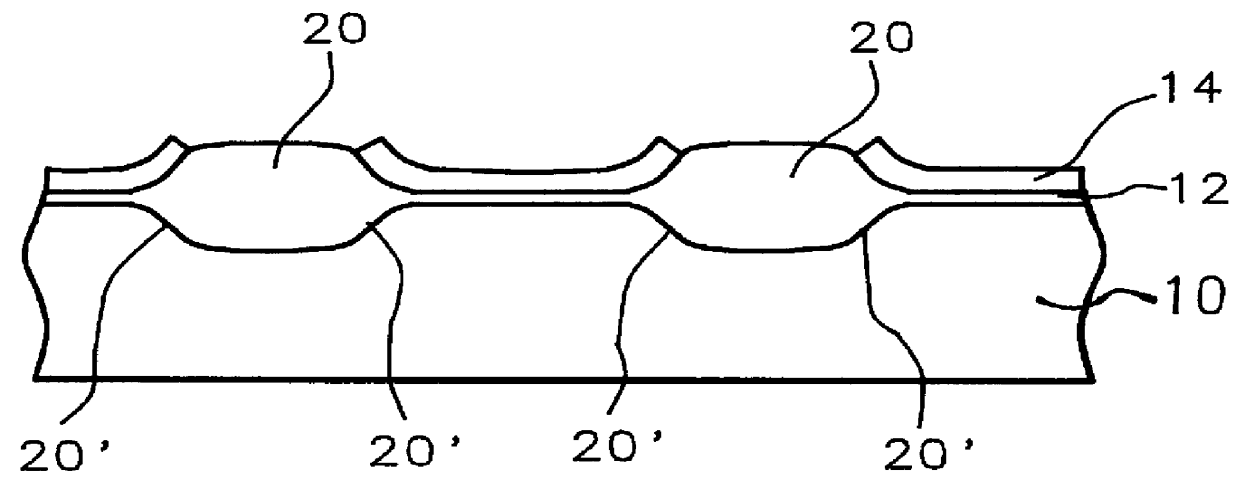
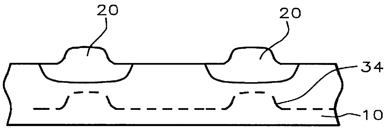
Silicon substrates were processed having DRAM cells with the conventional LOCOS process, as shown by the prior art of FIG. 1, and the modified field oxide, as shown in FIG. 5. Both field oxides were grown to a thickness of 2600 Angstroms. After forming the sidewall insulating portions 22' to form the modified field oxide (FIG. 5), both field oxide structures were implanted with boron at a dose of 4.5 E 12 ions / cm.sup.2. The threshold voltage (V.sub.th) of both field oxide structures was measured by forming a gate electrode over the field oxides between adjacent device areas, which serves as the source / drain areas for this field oxide MOSFET. The threshold voltages were determined by measuring the source / drain current as a function of the gate voltage. The conventional field oxide had a V.sub.th of 8.21 volts, and the modified field oxide had a V.sub.th greater than 10 volts, which is an improvement of at least 22% This clearly demonstrates the improved V.sub.th for the modified fiel...


PUM


Abstract

A method and structure for forming a modified field oxide region having increased field oxide threshold voltages (Vth) and / or reduced leakage currents between adjacent device areas is achieved. The method involves forming a field oxide using the conventional local oxidation of silicon (LOCOS) using a patterned silicon nitride layer as a barrier to oxidation. After forming the LOCOS field oxide by thermal oxidation and removing the silicon nitride, a conformal insulating layer composed of silicon oxide is deposited and anisotropically etched back to form sidewall insulating portions over the bird's beak on the edge of the LOCOS field oxide, thereby forming a new modified field oxide. P-channel implants are formed in the device areas. Then a second implant is used to implant through the modified field oxide to provide channel-stop regions with modified profiles that increase the field oxide Vth and / or reduce leakage current between device areas. This improved field oxide / channel-stop structure is particularly useful for reducing the leakage current on DRAM cells thereby increasing the refresh cycle times.

Description

(1) Field of the InventionThe present invention relates in general to the fabrication of semiconductor devices for integrated circuits, and more particularly to a method for forming a modified field oxide (FOX) isolation that increases the field oxide threshold voltages (V.sub.th) for a specific channel-stop implant dose under the FOX. Alternatively, the V.sub.th can be maintained at a constant value while the channel-stop implant dose can be reduced, which results in lower leakage currents between device areas. The method is particularly useful for dynamic random access memory (DRAM) for decreasing leakage currents and thereby increasing the refresh cycle times for storage capacitors.(2) Description of the Prior ArtIn the fabrication of semiconductor circuits, field oxide regions are formed in and on the silicon substrate (wafer) to surround and electrically isolate the device areas. One of the most common and cost-effective methods of forming this field oxide isolation in the semi...

Claims


Application Information

Patent Timeline
Patent Type & Authority Patents(United States)
IPC IPC(8): H01L21/02H01L21/762H01L21/70H01L21/32
CPCH01L21/76202H01L21/32
Inventor YOO, CHUE-SANSHIH, CHENG-YEH
Owner TAIWAN SEMICON MFG CO LTD
Why Eureka
Try Eureka