Solar cell and fabrication method thereof

Inactive Publication Date: 2000-10-10
SHARP KK
View PDF7 Cites 70 Cited by
  • Summary
  • Abstract
  • Description
  • Claims
  • Application Information

AI Technical Summary

Benefits of technology

The advantage of the present invention will be described hereinafter with a solar cell employing a single crystalline silicon substrate as an example.
Numbers of crystal defects can be formed within a crystal by implanting ions of silicon (.sup.28 Si.sup.+), for example, at an appropriate condition into the back side opposite to the light receiving surface and then applying an appropriate heat treatment. An amorphous layer is formed by the continuation of the crystal defects. Such a structure having the defects allows, light of a long wavelength that could previously not be absorbed effectively at the proximity of the light receiving surface and within the bulk, to be converted photoelectrically. The ideal silicon band gap is 1.12 eV. This corresponds to approximately 1.1 .mu.m when converted into wavelength. In principle, light of a wavelength greater than this wavelength cannot be converted photoelectrically in the solar cell. Light of a longer wavelength passes through outside the cell, or is converted into heat as shown in FIG. 7.
FIG. 7 shows the band of the portion where a defect layer is not present. The light of a short wavelength is represented by h.sub.v >E.sub.g. Holes excited by the short wavelength arrive at the conduction band. Light of a long wavelength represented by h.sub.v <E.sub.g do not contribute to photoelectric conversion. Such light is passing through outside the cell or i

Problems solved by technology

From the standpoint of effective usage of incident energy, there is a problem that long wavelength light is not utilized and lost, though light of the relatively short wavelength portion of the solar energy is substantially entirely converted photoelectrically at the proximity of the light receiving surface of the solar cell.
However, it is generally difficult to alter the band g

Method used


Image

  • Solar cell and fabrication method thereof
  • Solar cell and fabrication method thereof
  • Solar cell and fabrication method thereof

Examples


first embodiment

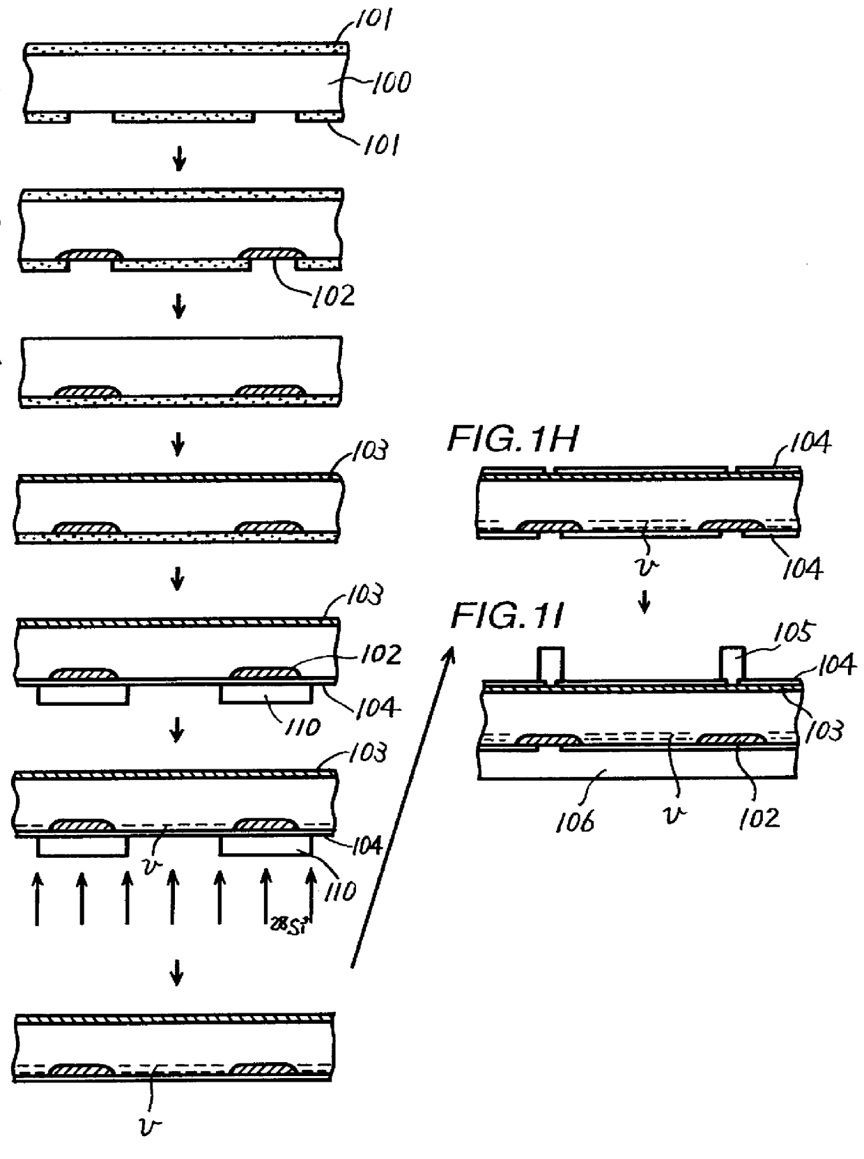
FIGS. 1A-1I are showing respective steps for fabricating a solar cell according to the present invention.

As shown in FIG. 1A, a single crystalline substrate (wafer) 100 including boron of approximately 1.times.10.sup.15 cm.sup.-3 and having a thickness of 30-500 .mu.m is prepared. At the back surface, p type diffusion layers such as of high concentration p type of at least 1.times.10.sup.17 cm.sup.-3 are locally formed. Both sides of the front surface and the back surface are covered with a mask material 101 such as a silicon oxide film. Holes in the mask material at the back surface are formed in an island-like manner by photolithography and etching technique.

As shown in FIG. 1B, the wafer is heated at the temperature of 500-1200.degree. C. in an atmosphere of the mixture of BBr.sub.3 gas and oxygen. An oxide including boron of high concentration is formed all over the surface of the wafer. By solid-phase diffusion therefrom, boron of high concentration is implanted only into the n...
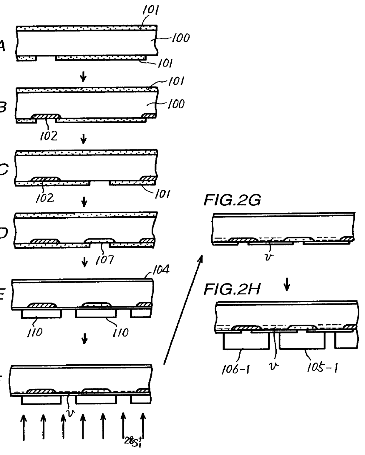
second embodiment

As a modification of the present invention, an n type diffusion layer can be formed at the front surface to provide an N electrode.

The fabrication method thereof is similar to that of the second embodiment.

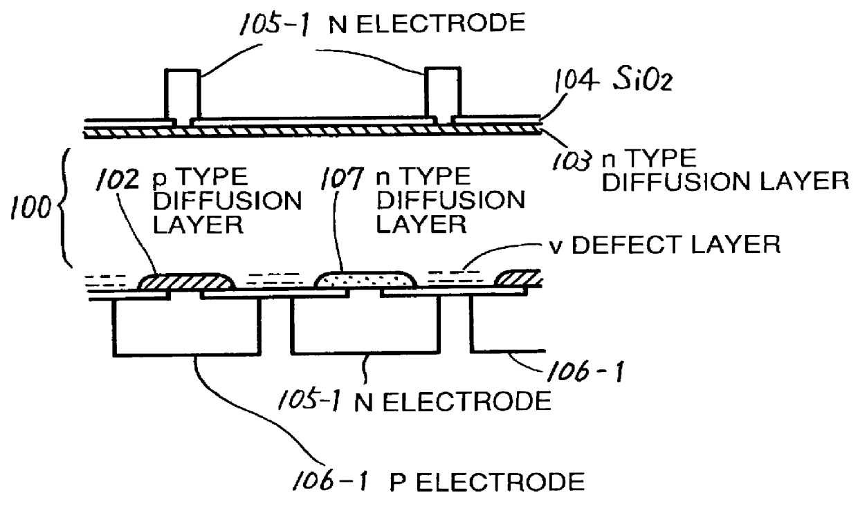
After the island-like p type diffusion layers of FIG. 2B are formed, the oxide film and mask material are removed from the surface of the wafer. High concentration n type diffusion layers of at least 1.times.10.sup.18 cm.sup.-3 are formed all over the light receiving surface and at local regions of the non-light receiving surface. Then, only the back surface is covered with a mask material. Holes are formed in the mask material by photolithography and etching at the region between the p type diffusion layers formed at the back surface side. The wafer is heated at the temperature of 500-1200.degree. C. in an atmosphere of the mixture of POCl.sub.3 gas and oxygen. As a result, an oxide including phosphorus of high concentration is formed all over the surface of the wafer. By solid-p...


PUM


Abstract

In a solar cell, a crystal defect layer by ion implantation or an amorphous layer by ion implantation is formed between p type diffusion layers provided in an island-like manner at a side opposite to a light receiving surface of a low concentration p type semiconductor single crystalline substrate. The element of the ion implantation may be at least one selected from the group consisting of hydrogen, silicon, germanium, fluorine, oxygen and carbon. The constituent substance of the semiconductor substrate, such as Si is preferably used for the ion implantation. In such a solar cell structure having the crystal defect or amorphous layer, relatively long wavelength light that could not effectively be utilized in the prior art solar cell may be utilized so that the photoelectric conversion efficiency may be improved.

Description

BACKGROUND OF THE INVENTION1. Field of the InventionThe present invention relates to the improvement of a solar cell and a fabrication method thereof.2. Description of the Background ArtIn general, a conventional solar cell has a structure as shown in FIG. 9, for example. The fabrication process is set forth in the following. In the present specification, the light receiving surface or side is referred to as the front surface or side and the opposite surface or side is referred to as the back surface or side.As shown in FIG. 9A, a single crystalline silicon substrate (wafer) 100 having a thickness of 30-500 .mu.m and including boron of approximately 1.times.10.sup.15 cm.sup.-3 is provided. A polycrystalline silicon substrate may also be used. A p type diffusion layer having high concentration of at least 1.times.10.sup.17 cm.sup.-3 is locally formed at the back surface. This portion becomes the local BSF (Back Surface Field) layer. The fabrication method includes the steps of coveri...

Claims


Application Information

Patent Timeline
IPC IPC(8): H01L31/0224H01L31/0352H01L31/0248H01L31/06H01L31/036H01L31/068H01L31/18H01L31/04H01L31/061
CPCH01L31/022425H01L31/036H01L31/068H01L31/022441H01L31/061H01L31/0682H01L31/1804Y02E10/547Y02E10/548Y02P70/50
Inventor NAKAMURA, KAZUYO
Owner SHARP KK
Why Eureka
Try Eureka