

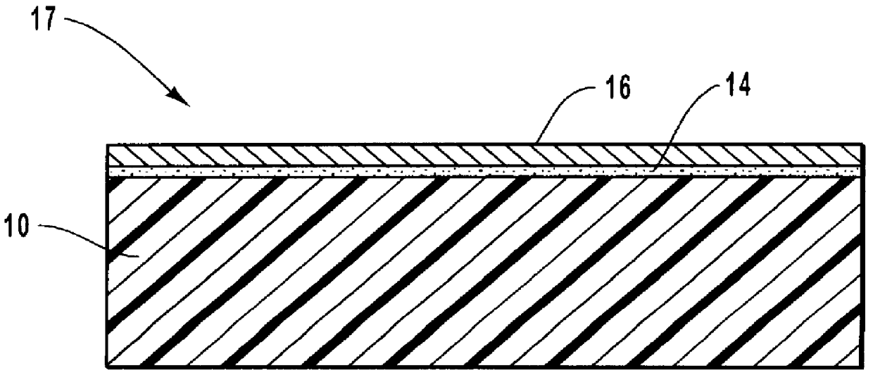
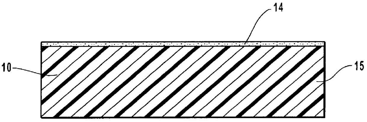
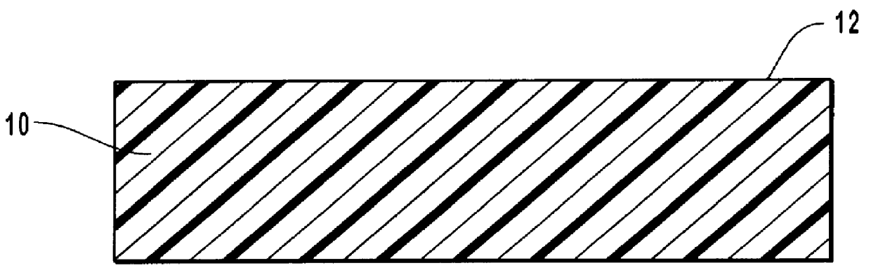
Polymeric optical substrate method of treatment
a polymer optical substrate and polymer technology, applied in the field of optical components, can solve the problems of easy scratching of coatings, premature peeling or delamination of coatings from the substrates, and difficult adhesion of optical coatings to these and other polymeric optical substrates, so as to increase the young's modulus and hardness, and increase the resistance to acetone damage
- Summary
- Abstract
- Description
- Claims
- Application Information
AI Technical Summary
Benefits of technology
Problems solved by technology
Method used
Image

Examples
example 2
Testing of Optical Substrates Comprising Film Deposited on PMMA Substrates Pretreated with Direct He Exposure
Rectangular plates of PMMA molded by reactive injection molding which were 2.5 millimeters thick, 75.times.15 mm in area were placed in system 18 on substrate holder / electrode 22 (18 cm in diameter) shown diagrammatically in FIG. 4. After turbomolecularly pumping the reactor down to a base pressure of 10.sup.-4 Torr, a helium gas was admitted using Sierra (Model 840) mass flow controllers, and the desired pressure was adjusted using a throttling valve and an MKS-Baratron capacitance pressure gauge.
Microwave power was supplied from a 2.45 GHz generator, and it was coupled to the reactor from a 30 cm long microwave periodic slow wave structure through a fused silica window 28 (located about 4 cm in front of each substrate). The substrate holder 22 was capacitively coupled to a radio frequency (RF, 13.56 MHz) power supply 30. The negative dc substrate-bias...
example 3
Testing of Optical Substrate Comprising Film Deposited on PMMA Substrate Pretreated with Direct He / N.sub.2 Exposure
An injection molded rectangular plate of PMMA was pretreated as described in the pretreatment method of Example 2 except that the PMMA plate was subjected to direct exposure of helium gas plasma for fifteen minutes, then direct exposure of nitrogen gas plasma for three minutes.
2. Coating and Testing Method:
An amorphous silicon nitride film was then deposited on the plate according to the coating method discussed above in Example 2, after which the resulting optical component was then tested as described in Example 2.
3. Test Results:
As shown in Table 3, the optical component demonstrated only trace delamination, indicating an improvement over the untreated samples of Example 1. The sample was visually clear.
example 4
Testing of Optical Substrates Comprising Film Deposited on PMMA Substrates Pretreated with Remote H.sub.2 Exposure
Rectangular plates of PMMA molded by reactive injection molding which were 2.5 millimeters thick, 75.times.15 mm in area were placed into a sample chamber of a double cavity system. The sample chamber was then pumped down to 10.sup.-6 Torr. Each sample was separated by a MgF.sub.2 filter window with a cut-off wavelength of 114 nm from the active plasma zone, such that wavelengths below 114 nm would not penetrate the window into the sample. An H.sub.2 plasma source was placed about 80 cm from the sample in the plasma chamber with the window separating the sample in the sample chamber from the plasma source in the plasma chamber. A microwave power of about 300 W was used, with a flow rate of about 10 sccm and a pressure of about 100 mtorr within the plasma chamber.
2. Coating and Testing Method:
Following pretreatment, the substrates were exposed to la...
PUM
| Property | Measurement | Unit |
|---|---|---|
| Thickness | aaaaa | aaaaa |
| Thickness | aaaaa | aaaaa |
| Percent by atom | aaaaa | aaaaa |
Abstract
Description
Claims
Application Information