Organic electroluminescent elements

a technology of electroluminescent elements and organic materials, applied in the direction of discharge tubes/lamp details, discharge tubes luminescnet screens, other domestic articles, etc., can solve the problems of short light emission life, low storage robustness and reliability, low light emission efficiency, current leakage, etc., to improve hole mobility, optimize hole injection efficiency, and improve the effect of thin film property

Inactive Publication Date: 2002-02-05
FUTABA CORPORATION
View PDF14 Cites 83 Cited by
  • Summary
  • Abstract
  • Description
  • Claims
  • Application Information

AI Technical Summary

Benefits of technology

With the organic EL device of the invention wherein the compound represented by formula (I) is used for a hole injecting layer or a hole injecting and transporting layer, it is possible to achieve consistent and uniform light emission due to an improved thin film property. The organic EL device of the invention also remains stable or uncrystallized over a period of 1 year or longer in the air. The aforesaid compound is characterized by having in its molecular structure a phenylenediamine skeleton to optimize hole injection efficiency and a benzidine skeleton (biphenyldiamine) and a skeleton having diamines with respect to a plurality of phenylenes to improve Hole mobility. Further, the organic EL device of the invention can stand up to high-temperature driving, and can efficiently emit light at a low driving voltage and a small driving current. Furthermore, when the organic EL device of the invention is continuously driven, there is only a slight or limited increase in the driving voltage. It is here to be noted that the EL device of the invention has a light emission maximum wavelength of the order of 400 to 700 nm.
FIG. 1 is a general schematic illustrative of one exemplary architecture of the organic EL device of the invention.
FIG. 2 is a .sup.1 H-NMR spectral diagram for synthesis

Problems solved by technology

On the other hand, problems with the organic EL device are that its light emission life is short, and its storage robustness and reliability are low for the following reasons.
When an organic thin film interface with ITO or the like is roughened, too, crystal grains manifest themselves and grow greatly, resulting in a light emission efficiency drop and current leakage which eventually lead to non-emission.
This is also a leading cause of local non-emitting spots, i.e., dark spots.
However, when these metals react with atmospheric moisture or oxygen or the organic layer peels off the electron injecting electrode, it is impossible to inject holes.
Especially when a high-molecular compound is formed into film as by spin coating, solvent residues after film formation, moisture and decomposed products accelerate the oxidation reaction of the electrode, and causes the delamination of the electrode, resulting in local non-emitting spots.
The generation of heat is unavoidable because a current is passed through the organic compound and so the organic compound must be placed in a high field strength.
The heat then gives rise to the melting, crystallization, and thermal decomposition of the organic compound, resulting in a deterioration and breakdown of the device.
Upon passing a current through the organic material, the organic material degrades, resulting in defects such as current or exciton traps.
These defects in turn cause a deterioration of the device such as a driving voltage increase or a luminance drop
In some cases, several problems arise; an inhomogeneous organic layer is formed on the hole injecting electrode, and no good interface can be formed.
Thus, the oxidation of the electrode proceeds rapidly, causing a striking luminance drop or a noticeable driving voltage increase.
Problems with the evaporated polythiophene film are that the reproducibility of fabrication of good devices is low due to large variations in the degree of polymerization of polythiophene and large fluctuations in polythiophene during evaporation, and the surface of ITO cannot be fully denatured due to difficulty involved in making polythiophene thick because the polythiophene itself has light absorption in a visible light region.
However, it is found that sufficient heat resistance is not obtained, and that a homogeneous and stable film cannot be obtained on a hole injecting electrode during high-temperature storage.

Method used


Image

  • Organic electroluminescent elements
  • Organic electroluminescent elements
  • Organic electroluminescent elements

Examples


synthesis example 1

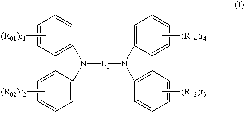
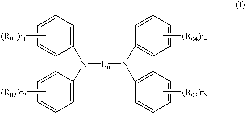
Synthesis of N,N'-diphenyl-N,N'-bis[N-phenyl-N-3-tolyl(4-aminophenyl)]benzidine (HIM33: compound No. 3)

In a 200 ml reaction vessel 26 grams of N,N-diphenyl-1,4-phenylenediamine and 22 grams of 3-iodotoluene were heated together with 0.3 grams of activated copper powders, 50 grams of potassium carbonate and 50 ml of decalin at an oil bath temperature of 200.degree. C. for 24 hours in an Ar atmosphere. After the completion of the reaction, the reaction solution was filtrated with the addition of 100 ml of toluene thereto, thereby removing insolubles. The filtrate was washed with water, and dried over sodium sulfate. Following this, the solvent was removed by distillation from the filtrate, and the residue was purified twice by means of a silica gel column (using a mixed solvent of n-hexane and toluene as a developing solvent), thereby obtaining 17 grams of N,N'-diphenyl-N-(3-tolyl)-1,4-phenylenediamine.

Then, in a 200 ml reaction vessel 10 grams of N,N'-diphenyl-N-(3-tolyl)-1,4-phenyle...

synthesis example 2

Synthesis of N,N'-diphenyl-N,N'-bis[N-phenyl-N-4-tolyl(4-aminophenyl)]benzidine (HIM34: compound No. 2)

N,N'-diphenyl-N,N'-bis[N-phenyl-N-4-tolyl(4-aminophenyl)]benzidine referred to below as HIM34 was obtained as in synthesis example 1 with the exception that 4-iodotoluene was used in place of 3-iodotoluene. ##STR957##

Mass spectrometry: m / e 850(M.sup.+)

.sup.1 H-NMR spectra are shown in FIG. 5.

.sup.13 C-NMR spectra are shown in FIG. 6.

Infrared absorption spectra are shown in FIG. 7.

Differential scanning calorimetry (DSC)

Melting point: unmeasurable because of amorphism

Glass transition temperature (DSC): 107.degree. C.

synthesis example 3

Synthesis of N,N'-diphenyl-N,N'-bis[N-phenyl-N-4-tolyl(4-aminophenyl)]benzidine (HIM38: compound No. 16)

N,N'-diphenyl-N,N'-bis[N-phenyl-N-4-tolyl(4-aminophenyl)]benzidine referred to below as HIM38 was obtained as in synthesis example 1 with the exception that 4-iodonaphthalene was used in place of 3-iodotoluene. ##STR958##

Mass spectrometry: m / e 922(M.sup.+)

.sup.1 H-NMR spectra are shown in FIG. 8.

.sup.13 C-NMR spectra are shown in FIG. 9.

Infrared absorption spectra are shown in FIG. 10.

Differential scanning calorimetry (DSC)

Melting point: unmeasurable because of amorphism

Glass transition temperature (DSC): 125.degree. C.


PUM

PropertyMeasurementUnit
thicknessaaaaaaaaaa
light emission maximum wavelengthaaaaaaaaaa
thicknessaaaaaaaaaa

Abstract

An organic EL device comprising a cathode, an anode, and at least one organic compound layer containing an organic compound represented by formula (I):where L0 is any one of o-, p-, and m-phenylene groups which have two, three or four rings and which have a substituent with the proviso that when L0 is a phenylene group having four rings, the phenylene group may have an unsubstituted or substituted aminophenyl group somewhere therein, and at least one of R01, R02, R03 and R04 is any one of the following groups:where R1, R12, R13, R14, R15, R16 and R17 are each a substituted or unsubstituted aryl group, and r1, r2, r3 and r4 are each an integer of 0 to 5 with the proviso that r1+r2+r3+r4>=1.

Description

The present invention relates generally to an organic EL (electroluminescent) device, and specifically to a device which emits light upon the application of an electric field to a thin film of multilayered structure. More specifically, the present invention is concerned with an organic electro-luminescent light emission device including a hole injecting layer comprising a specific triarylamine polymer, so that low driving voltage, stable light emission, high quality display images and high heat resistance are achievable.BACKGROUND TECHNIQUEAn organic EL device comprises a thin film containing a fluorescent organic compound interleaved between an electron injecting electrode (cathode) and a hole injecting electrode (anode), and emits light making use of light emissions (fluorescence and phosphorescence) upon deactivation of excitons which are generated by injecting electrons and holes in the thin film for their recombination.Features of the organic EL device are that surface light em...

Claims


Application Information

Patent Timeline
Patent Type & Authority Patents(United States)
IPC IPC(8): C09K11/06H01L51/00H01L51/30H01L51/50H05B33/12H05B33/14
CPCC09K11/06C09K2211/1003C09K2211/1007C09K2211/1011C09K2211/1014H05B33/12H05B33/14Y10S428/917H10K85/622H10K85/623H10K85/626H10K85/633H10K85/615H10K85/631H10K85/324H10K50/11H10K2102/103
Inventor INOUE TETSUSHIAOTANI JUNJIFUJITA TETSUJIENDO HIROYUKI
Owner FUTABA CORPORATION
Why Eureka
Try Eureka