
Metal complex solution, photosensitive metal complex solution, and method for forming metallic oxide films

a technology of complex solution and metal, applied in the direction of group 3/13 element organic compounds, nuclear engineering, railway components, etc., can solve the problems of insufficient quality of metallic oxide films, complex and expensive film deposition systems used in this process, disadvantageous conventional sputtering process, etc., and achieve the effect of lowering the resolution of the pattern

Inactive Publication Date: 2002-05-14
DAI NIPPON PRINTING CO LTD
View PDF31 Cites 23 Cited by
  • Summary
  • Abstract
  • Description
  • Claims
  • Application Information

AI Technical Summary

Benefits of technology

According to the present invention, it becomes possible to form high-quality metallic oxide films, or transparent conducting films, such as ITO films, having low electrical resistance and high transparency on substrates by a method of application utilizing the so-called sol-gel process.
It is more preferable to use a lower alkoxide such as methoxide, ethoxide, n-propoxide, isopropoxide, n-butoxide or isobutoxide. This is because, when such a lower alkoxide is used, an ITO film articularly excellent in electrical conductivity and transparency can be obtained.
By adding a Sn alkoxide to the above-obtained In complex solution, an In--Sn complex solution of the present invention can be obtained. In the present invention, it is preferable to further heat-treat this mixture at a temperature of approximately 80 to 160.degree. C. for approximately 1 to 4 hours. Although the details are unknown, it is considered that complexation further occurs between the In complex and the Sn alkoxide by this heat treatment. Although some precipitates separate out by the heat treatment, the solution is sufficiently stable, and can be stored for a long period of time. By removing, when necessary, the impurities separated, an In--Sn complex solution of the present invention which is substantially transparent can be obtained.
By the energy of the light applied to the transparent conducting film, grain boundaries in the film are connected to one another, so that the mobility of conduction electrons in the film is enhanced. The electrical resistance of the transparent conducting film is thus lowered. The level of this energy can be properly decided depending upon the materials used for forming the transparent conducting film, the thickness of the film, the light source to be used, and the intended use of the film.
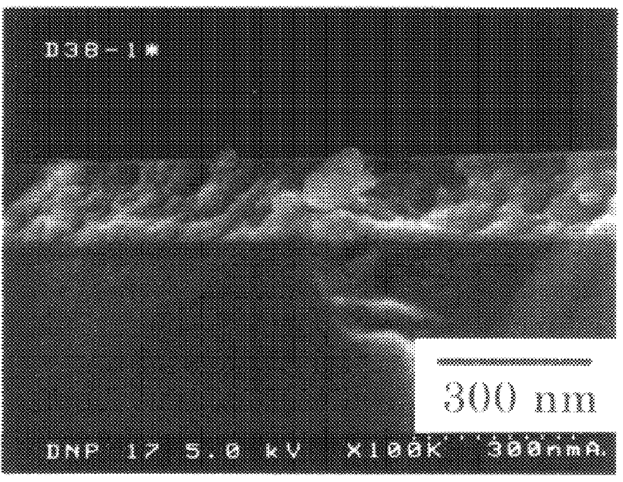
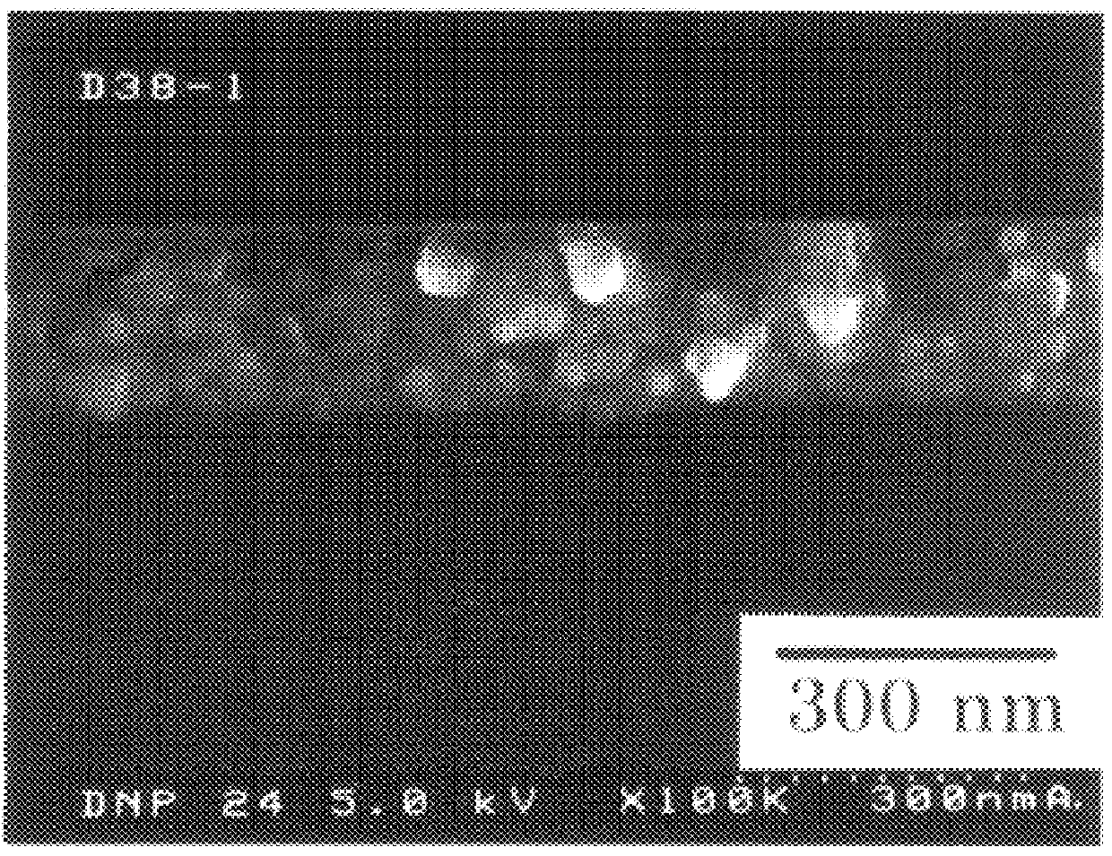
Through the above-described steps, a patterned transparent conducting film (ITO film) accurately corresponding, to the pattern of a photomask used is formed on a substrate. The ITO film thus obtained is excellent in transparency and also in electrical conductivity like ITO films obtainable by the conventional vacuum vapor deposition, sputtering or CDV process. Therefore, according to the present invention, it becomes possible to form patterned transparent conducting films useful for various uses by a simple process without using an expensive system.
In Examples of the present invention, pattern-wise exposure is conducted by using a photoresist to make a difference in solubility to a developer between the exposed portions and unexposed portions on the coating. A fine pattern is thus formed after development. At this time, when the exposure energy is made smaller than the above-described value, it becomes difficult to form a fine pattern. On the other hand, when the exposure energy is made greater than the above-described value, the shape of the edge of the resulting fine pattern is impaired (the edge becomes undulated). As a result, the resolution of the pattern is lowered.

Problems solved by technology

The above-described conventional sputtering process is disadvantageous from the view points of production cost and mass-productivity because the film deposition system for use in this process is complicated and also expensive.
However, those metallic oxide films, especially transparent conducting films which are formed by these methods of application are still insufficient in their qualities.
Namely, there are such practical problems that the qualities of the metallic oxide films are unsatisfactory and that, since the transparent conducting films formed have high electrical resistance, they cannot be used for electrodes or the like to be used for display elements, etc. when electrical conductivity is taken into consideration.
The above-described conventional method for forming patterned metallic oxide films or transparent conducting films is a complicated and long process consisting of two film-forming steps of forming a metallic oxide film or transparent conducting film and a resist layer, one step of exposure, and three wet chemical conversion treatment steps of developing the resist layer, removing the same, and etching the metallic oxide film or transparent conducting film.
This method is thus disadvantageous when considering production cost and non-defective rate.

Method used


Image

  • Metal complex solution, photosensitive metal complex solution, and method for forming metallic oxide films
  • Metal complex solution, photosensitive metal complex solution, and method for forming metallic oxide films

Examples


example 1

1. Preparation of In--Sn Complex Solution

A 1,000 ml three-necked flask equipped with a mechanical stirrer, a Dimroth condenser, a thermometer, and silicone rubber stoppers was prepared. The flask was unstoppered, and 3.2 mol of acetic acid was placed in the flask.

0.04 mol of indium oxide (purity: 99.999%) was added to the flask with stirring the acetic acid in the flask, and the temperature of the mixture was raised, with stirring, to 100.degree. C. over a period of 30 minutes by using an oil bath. The mixture was heated under reflux at the temperature for 5 hours, and then cooled to room temperature.

The solution contained in the above flask was transferred to a 500 ml egg-plant type flask, and concentrated to 50.1 g by using a rotary evaporator at a temperature of 70.degree. C. under a pressure of 30 mmHg.

This concentrate was transferred to a 1,000 ml three-necked flask equipped with a mechanical stirrer, a Dimroth condenser, a thermometer and silicone rubber stoppers, and stirred ...

example 2

A photosensitive In--Sn complex solution of the present invention was prepared in the same manner as in Example 1 except that 0.08 mol of triethanolamine used in Example 1 was replaced with 0.24 mol of acetylacetone. By the use of this complex solution, the substrate with a finely-patterned transparent conducting film was obtained in the same manner as in Example 1.

example3

A photosensitive In--Sn complex solution of the present invention was prepared in the same manner as in Example 1 except that 0.08 mol of triethanolamine used in Example 1 was replaced with 0.16 mol of diethanolamine. By the use of this complex solution, the substrate with a finely-patterned transparent conducting film was obtained in the same manner as in Example 1.


PUM

PropertyMeasurementUnit
temperatureaaaaaaaaaa

Abstract

A metal complex solution comprising an organic solvent, and a complex composed of an organic acid salt of at least one metal and an organic amine or organic ketone compound, dissolved in the organic solvent; a photosensitive metal complex solution comprising the metal complex solution, and a photosensitive resin added to the solution; and a method for forming metallic oxide films, using these solutions.

Description

1. Field of the InventionThe present invention relates to a metal complex solution, to a photosensitive metal complex solution, and to a method for forming metallic oxide films (including patterned metallic oxide films).2. Background ArtMetallic oxides have attracted attention from old times due to their thermal, optical, electrical, magnetic and mechanical properties, and conventionally have been applied to various uses in the field of industry. Especially in the field of recent electronic materials, transparent conducting films are used as antistatic materials, materials for heat ray cut-off filters, materials for ultraviolet light cut-off filters, magnetic-wave-shielding materials, materials for transparent electrodes to be used for liquid crystal displays, plasma displays, etc., and materials for producing deicing heaters to be used for window glasses, etc. Further, a variety of metallic oxide films are utilized for those uses which require neither transparency nor electrical co...

Claims


Application Information

Patent Timeline
Patent Type & Authority Patents(United States)
IPC IPC(8): G03F7/004C04B35/26C04B35/457C04B35/472C07F5/00C07F7/22G02F1/1343G03F7/40H01F41/24H01L31/18H01L51/52
CPCC04B35/2658C04B35/472C04B35/6264G03F7/0047H01F41/24H01L31/1884C04B35/457Y02E10/50C04B2235/3232C04B2235/3272C04B2235/3284C04B2235/3286C04B2235/3293C04B2235/3296C04B2235/441C04B2235/449C04B2235/768C04B2235/96C04B2235/9653G02F1/13439H01L51/5206C03C17/27C03C2217/212C03C2217/217C03C2217/231C03C2217/24C03C2217/948H10K50/81
Inventor MITAMURA, SATOSHI
Owner DAI NIPPON PRINTING CO LTD
Learn More