GaN single crystal substrate and method of producing same

a single crystal substrate and substrate technology, applied in the field of single crystal substrates, can solve the problems of high defect density, sapphire substrates with another drawback from the mechanical viewpoint, and the best sapphire substrate still has a problem,

Inactive Publication Date: 2002-07-02
SUMITOMO ELECTRIC IND LTD
View PDF6 Cites 284 Cited by
  • Summary
  • Abstract
  • Description
  • Claims
  • Application Information

AI Technical Summary

Problems solved by technology

The best sapphire substrate still has a problem.
The high density of defects may be a problem on crystallography but is not a practical problem in the GaN-LEDs.
The sapphire substrate has another drawback from the mechanical viewpoint.
The high stability against chemicals is a drawback as well as a merit.
The most inconvenient matter is the lack of cleavage.
The lack of cleavage and the rigidity enhance the difficulty of dicing a GaN / sapphire wafer into plenty of device chips.
Rigidity and non-cleavage are the most serious difficulty of sapphire substrates.
However, this example is only on a laboratory scale.
Namely, difficulty lies at the production of SiC crystals.
The SiC substrate itself is still expensive.
The SiC will raise the cost of GaN / SiC devices.
In practice, the GaN / SiC devices have not been made on a large scale yet.
SiC is not matured to a practical material of substrates.
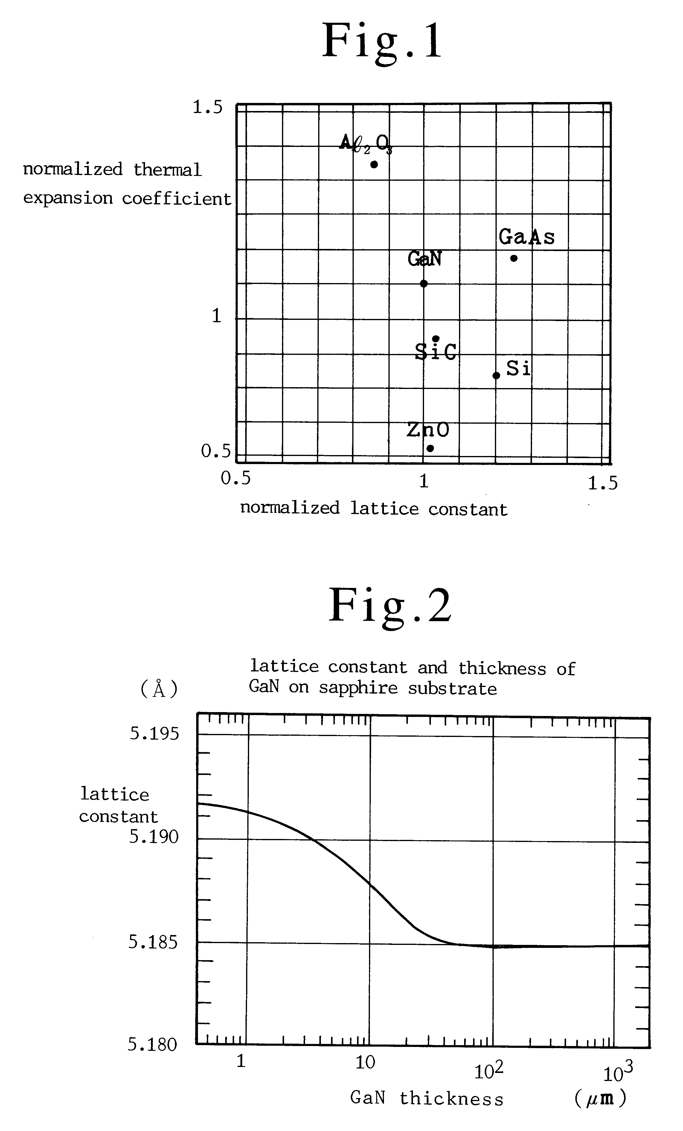
Cooling causes undesirable influences on the GaN films due to the difference of thermal expansion coefficients between the GaN films and the substrate.
The difference of thermal expansion coefficients between the films and the substrate causes a first problem of occurrence of thermal stress in the GaN films.
A further problem is the fact that the thermal expansion coefficient difference invites distortion of the substrate in the cooling process.
A third problem is impossibility of making a large complex GaN / sapphire substrate.
But, large distortion and big stress prevent manufactures from producing large GaN / sapphire wafers.
The GaAs substrate, however, had a serious drawback.
All the trials had failed in making a good GaN on a GaAs substrate wafer.
However, if the defects were reduced, the lifetime of GaN LEDs would be prolonged further.
Besides, GaN LDs don't have a long lifetime enough for practical use.
The improved GaN-LEDs are still suffering from the problem of non-cleavage.
Dicing the GaN / sapphire wafer into LED chips would be still a difficult process of a low yield due to the non-cleavage of the sapphire substrate.
The sapphire substrate would still have a large distortion.
The distortion would impede the wafer processes by the lithography.
The problem of the differences of the thermal expansion and the lattice constants is inherent in the use of the foreign material substrate.
However, wide GaN single crystals cannot be produced yet at present.
These methods are impotent for a material which does not take liquid phase by heating.
The space maintaining the ultrahigh pressure, however, is too narrow.
It is difficult to make a transparent, colorless GaN film due to the impurity. carbon.
Furthermore, the carbon atoms increase the carrier concentration (free electron concentration) and reduce the electron mobility.
These are the drawbacks of the MOC method.
The MOCVD method has an economical weak point of low yield, since a great amount of gases are utilized in the MOCVD.
When a thin film, e.g., an activation layer is formed, the poor efficiency may be negligible.
But when the object is a production of a thick substrate crystal, the low efficiency of gases would be a fatal drawback.
Besides the inefficient gas consumption, the MOCVD is also suffering from the carbon inclusion from the metallorganic compound.
GaN-type devices have been heteroepitaxially grown on sapphire single crystal substrates, since there is no technique of making a wide bulk GaN single crystal substrate.
A thick GaN wafer thicker than 1 mm would raise the cost.
The most important problem for the method of making GaN films is reduction of the distortion of substrate crystals.
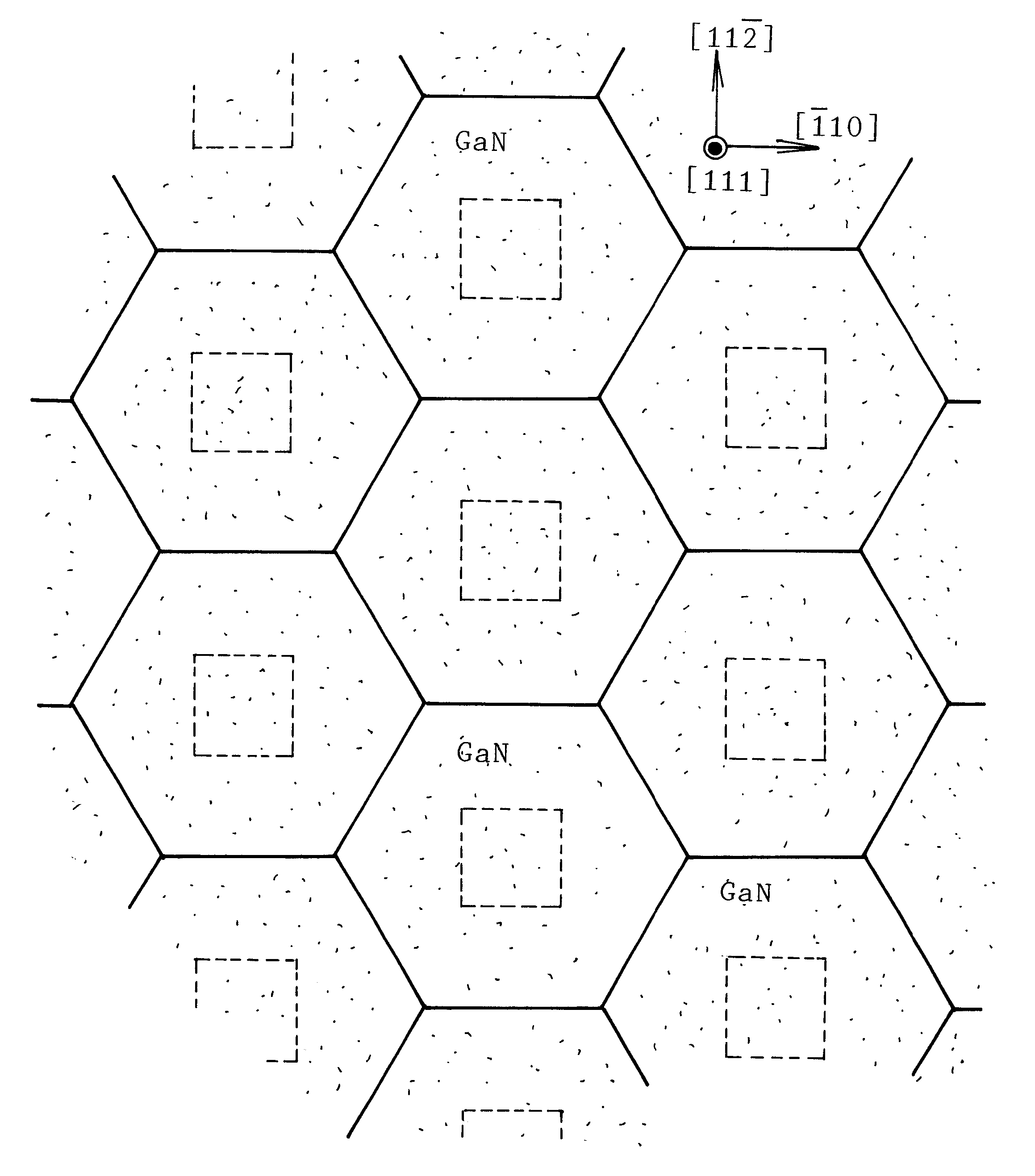
However, the inclusion of As is very little, since the mask and the buffer layers protect the GaN from the As pollution.
There is no means for eliminating only the sapphire substrate.
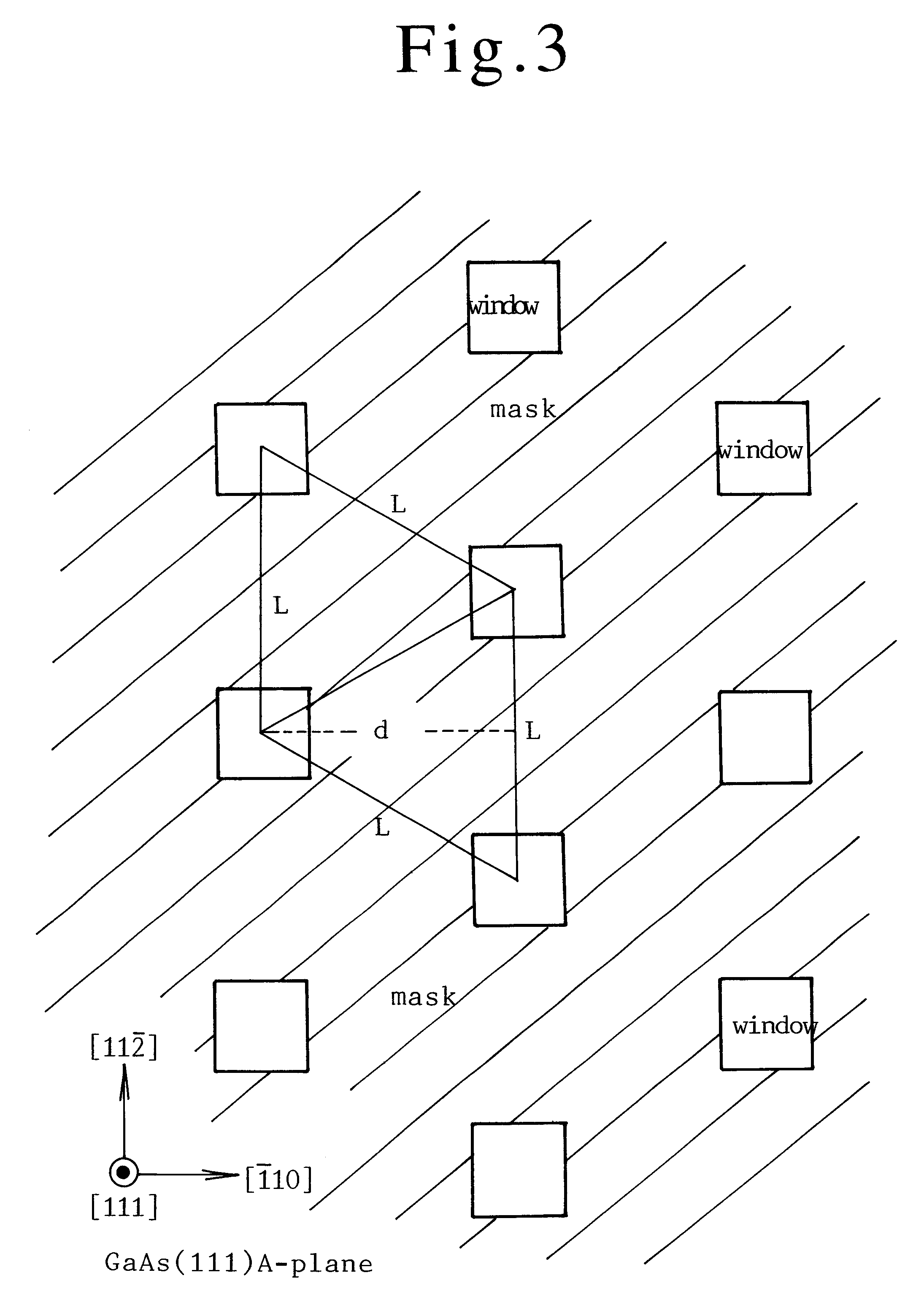
But the striped window type mask has a drawback of larger distortion and higher defect density than the dotted window type mask.
Otherwise, when low-purity materials are used and oxygen pressure is not regulated, non-doped GaN is suffering from high carrier density and low mobility.
Another serious problem is the distortion and the internal stress.
Large distortion prohibits photolithography or other wafer process from making devices on the GaN substrate.
Too large distortion forbids the photolithography.
But stress is an inner potential which refuses direct measurement.
The conventional sapphire substrate allows occurrence of plenty of piercing dislocations in the active layer which reduce the light power.
te is good. But category A has a drawback of large inte
rnal stress. The large internal stress invites cracks on
The surface state is bad.
In addition, the GaN grown directly on GaAs without masks has a very small distortion radius and strong internal stress, which breaks the GaN crystal itself

Method used


Image

  • GaN single crystal substrate and method of producing same
  • GaN single crystal substrate and method of producing same
  • GaN single crystal substrate and method of producing same

Examples


Embodiment Construction

7 (Anisotropy of the Internal Stress in Wafer)]

The anisotropy of internal stress is investigated for both the GaN wafers (.mu.) made by the striped window mask and the GaN wafers (.nu.) made by the dotted window mask.

Sample (.mu.) . . . 120 .mu.m average thick GaN wafers made by producing a GaAs striped window mask on a GaAs(111) wafer, piling GaN buffer layers and GaN epitaxial layers, and etching the GaAs substrate away.

Sample (.nu.) . . . 160 .mu.m average thick GaN wafers made by producing a dotted window mask (FIG. 3) on a GaAs(111) wafer, piling GaN buffer layers and GaN epitaxial layers, etching the GaAs substrate away.

Both samples are grown by the same conditions of a Ga partial pressure of 1.times.10.sup.-2 atm(1 kPa), a NH.sub.3 partial pressure of 0.24 atm (24 kPa), a growth time of 240 hour and a growth temperature of 970.degree. C. After the growth, the GaN substrates are cooled and taken out from the HVPE apparatus. The GaAs substrates are etched away for obtaining fre...


PUM

PropertyMeasurementUnit
thicknessaaaaaaaaaa
thicknessaaaaaaaaaa
absorption coefficientaaaaaaaaaa

Abstract

A freestanding GaN single crystal substrate is made by the steps of preparing a (111) GaAs single crystal substrate, forming a mask having periodically arranged windows on the (111) GaAs substrate, making thin GaN buffer layers on the GaAs substrate in the windows of the mask, growing a GaN epitaxial layer on the buffer layers and the mask by an HVPE or an MOC, eliminating the GaAs substrate and the mask away and obtaining a freestanding GaN single crystal substrate. The GaN single crystal has a diameter larger than 20 mm and a thickness more than 0.07 mm, being freestanding and substantially distortion-free.

Description

1. Field of the InventionThis invention relates to a GaN single crystal substrate for making blue light LEDs (light emitting diodes) or blue light LDs (laser diodes) based upon III-V group nitride (GaN-like) semiconductors.This application claims the priority of Japanese Patent Applications No.10-171276(171276 / 1998) filed on Jun. 18, 1998 and No.10-183446(183446 / 1998) filed on Jun. 30, 1998, which are incorporated herein by reference.2. Description of Prior ArtFIG. 1 shows the ratios of the lattice constant and the thermal expansion coefficient of the candidate materials for the substrate of growing GaN to those of GaN. Here, candidate substrates for GaN growth are sapphire (Al.sub.2 O.sub.3), silicon carbide (SiC), silicon (Si), gallium arsenide (GaAs) and zinc oxide (ZnO). The nitride semiconductor light source devices, or GaN-group light source devices have been produced by piling GaN or GaN-like films epitaxially upon a sapphire substrate (Al.sub.2 O.sub.3). The sapphire substra...

Claims


Application Information

Patent Timeline
Patent Type & Authority Patents(United States)
IPC IPC(8): C30B25/02H01L21/02H01L21/20H01L33/00H01L33/32
CPCC30B25/02C30B29/406C30B29/60H01L21/02395H01L21/02458H01L21/0254H01L21/02639H01L21/02647H01L21/02664H01L33/007H01L33/32H01L21/0262Y10T428/26H01L33/0079H01L33/0093
Inventor MOTOKI, KENSAKUOKAHISA, TAKUJIMATSUMOTO, NAOKINISHIMOTO, TATSUYA
Owner SUMITOMO ELECTRIC IND LTD
Why Eureka
Try Eureka