

Integrated circuit biochip microsystem
- Summary
- Abstract
- Description
- Claims
- Application Information
AI Technical Summary
Benefits of technology
Problems solved by technology
Method used
Image

Examples
example 1
5.1 Example 1
Nucleic Acid Biochip Integrated Device
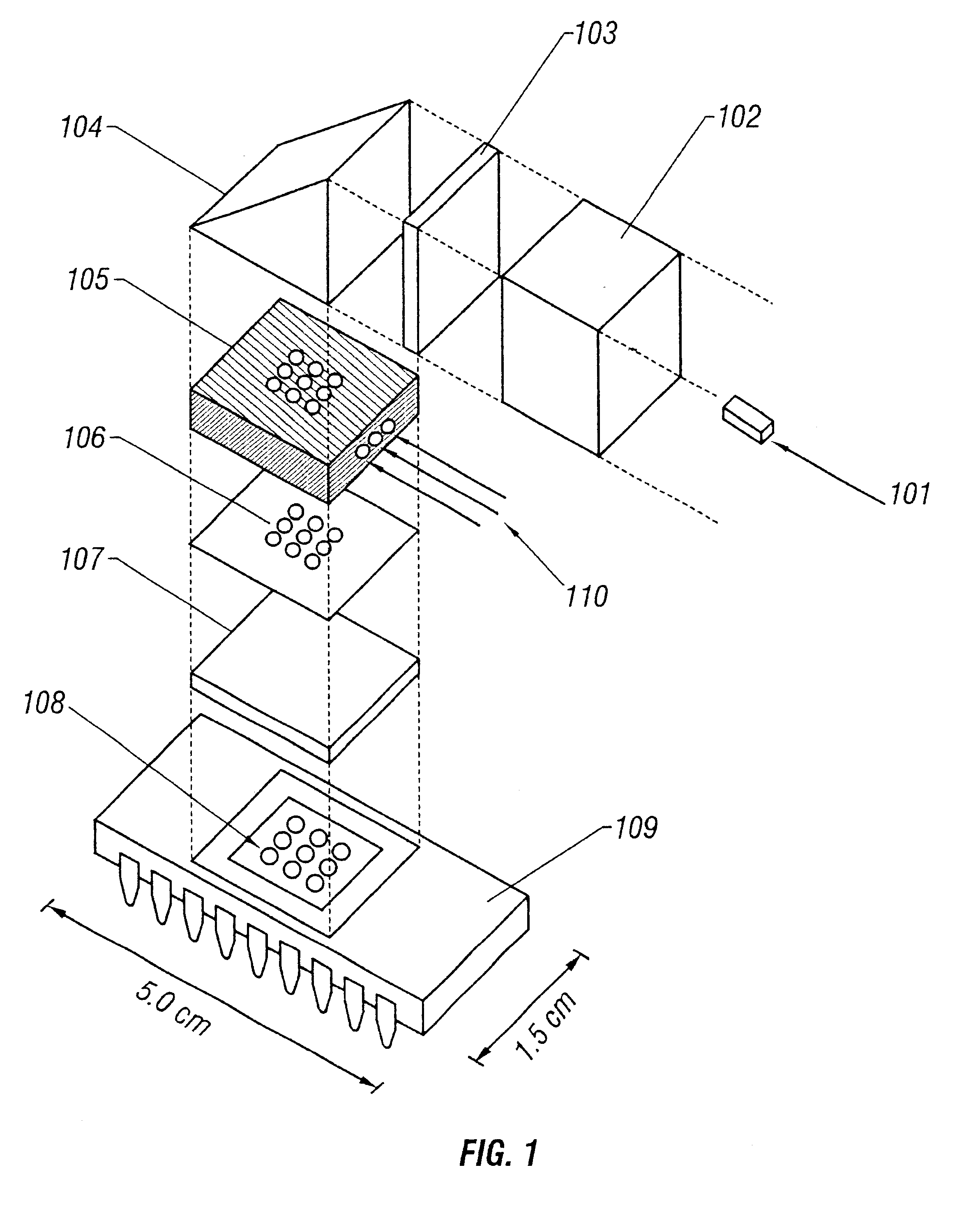
FIG. 1 shows an exploded, schematic, perspective view of an example of DNA biochip 109 that combines optical and electrical components. The components shown include a light source 101, optical element 102, filter 103, reflective optic 104, sampling platform 105 for receiving and delivering sample 110 onto spot arrays 106 on a substrate 111, filter 107, and an array of photodetectors 108.
The optical elements shown in FIG. 1 may be positioned separately from the biochip 109, but are preferably integral with the biochip. In the latter instance, a transparent shield or seal (e.g plate made with glass or quartz or plastic which is optically transparent at the wavelengths of interest for deletion) isolates the optical component from the biochemical components. Light from light source 101 travels through self-imaging optical element 102 (e.g defractive optics, binary optics or self-imaging optics systems that transform a point source into ...
example 2
5.2 Example 2
Optical Detector and Amplifier Circuit
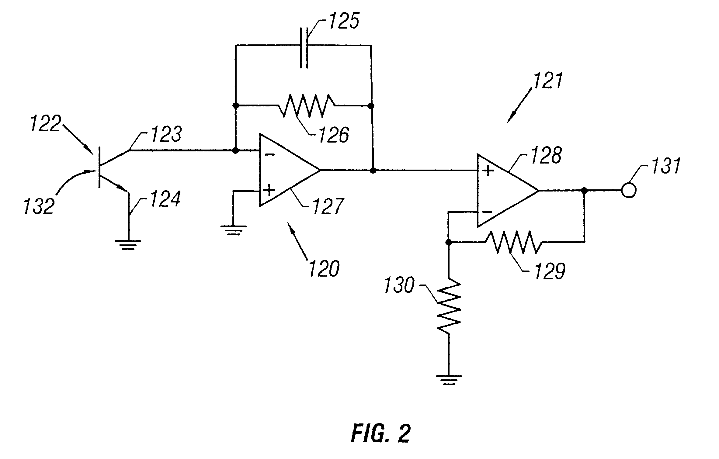
These optical detector and amplifier circuit shown in FIG. 2 may be implemented on an integrated circuit in order to convert an optical signal into an electrical signal suitable for data digitization and capture by a computer. The optical detector and amplifier includes a phototransistor 122 coupled to a transimpedence amplifier 120, which converts a current signal into a voltage signal and which is followed by an amplifier 121. The operational amplifier 127 in the transimpedence amplifier 120 is a two-stage, unbuffered amplifier.
In one embodiment, capacitor 125 has a value of 2 pF and resistor 126 has a value of 100 K.OMEGA.. The gain of amplifier 121 is equal to 1+(Resistance 129 / Resistance 130). Thus, in one specific embodiment for which the gain of amplifier 121 is 10, resistors 129 and 130 are chosen so that their ratio is 9. The circuit is compact (185 .mu.m.times.200 .mu.m), but has moderately high performance. It is designed...
example 3
5.3 Example 3
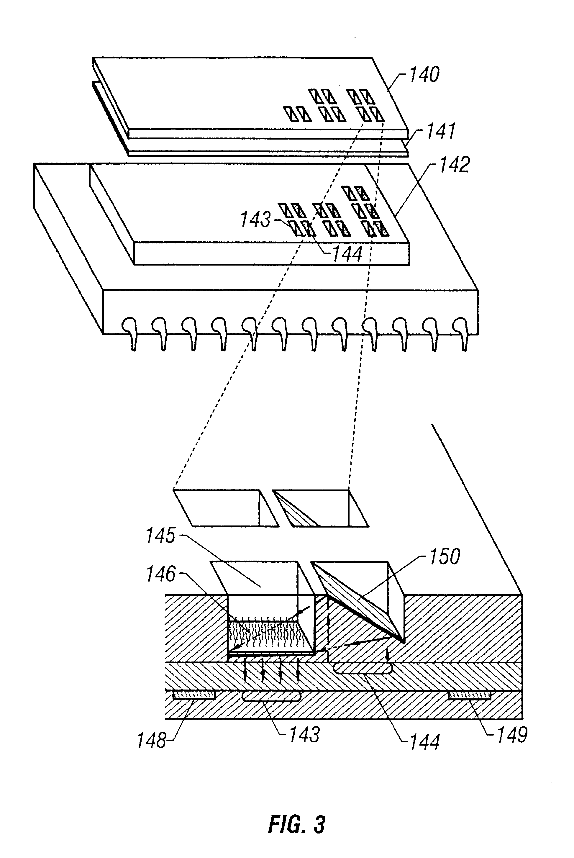
FIG. 3 shows a biochip having multiple arrays of exciting light sources and detectors. The biochip includes a sampling stage layer 140, a filter and lens stage layer 141, and a silicon die stage layer 142. Light from light source 144 driven by a driver circuit 149, see FIG. 30, is reflected from mirror coating 150. The mirror surface is designated such that the light beam from 144 is focused and directed to cover the area of the microchamber surface which contain the DNA probe or DNA sample. If luminescence is the signal being detected, the resulting light travels through an optional filter and lens stage 147 and is detected by the photodetector 143 and the associated signal processing electronics 148 such as the system shown in FIG. 9.
PUM
| Property | Measurement | Unit |
|---|---|---|
| Current | aaaaa | aaaaa |
| Transmission | aaaaa | aaaaa |
| Electric potential / voltage | aaaaa | aaaaa |
Abstract
Description
Claims
Application Information