Single crystal SiC composite material for producing a semiconductor device, and a method of producing the same

a composite material and single crystal technology, applied in the direction of polycrystalline material growth, silicon compounds, gel state, etc., can solve the problems of unstable substrate, easy warpage or deformation of semiconductor devices, and difficult to ensure thickness and strength which are requested

Inactive Publication Date: 2003-02-25
NISSIN ELECTRIC CO LTD
View PDF7 Cites 5 Cited by
  • Summary
  • Abstract
  • Description
  • Claims
  • Application Information

AI Technical Summary

Problems solved by technology

Therefore, the substrate is unstable.
Consequently, it is difficult to ensure the thickness and the strength which are requested in the use and handling of a material for producing a semiconductor device.
As a result, there arises a disadvantage that warpage or deformation easily occurs in a semiconductor device which is produced from a single crystal SiC material.
The thickness of such a single crystal SiC film is ins

Method used


Image

  • Single crystal SiC composite material for producing a semiconductor device, and a method of producing the same
  • Single crystal SiC composite material for producing a semiconductor device, and a method of producing the same
  • Single crystal SiC composite material for producing a semiconductor device, and a method of producing the same

Examples


Embodiment Construction

Hereinafter, an embodiment of the invention will be described with reference to the drawings.

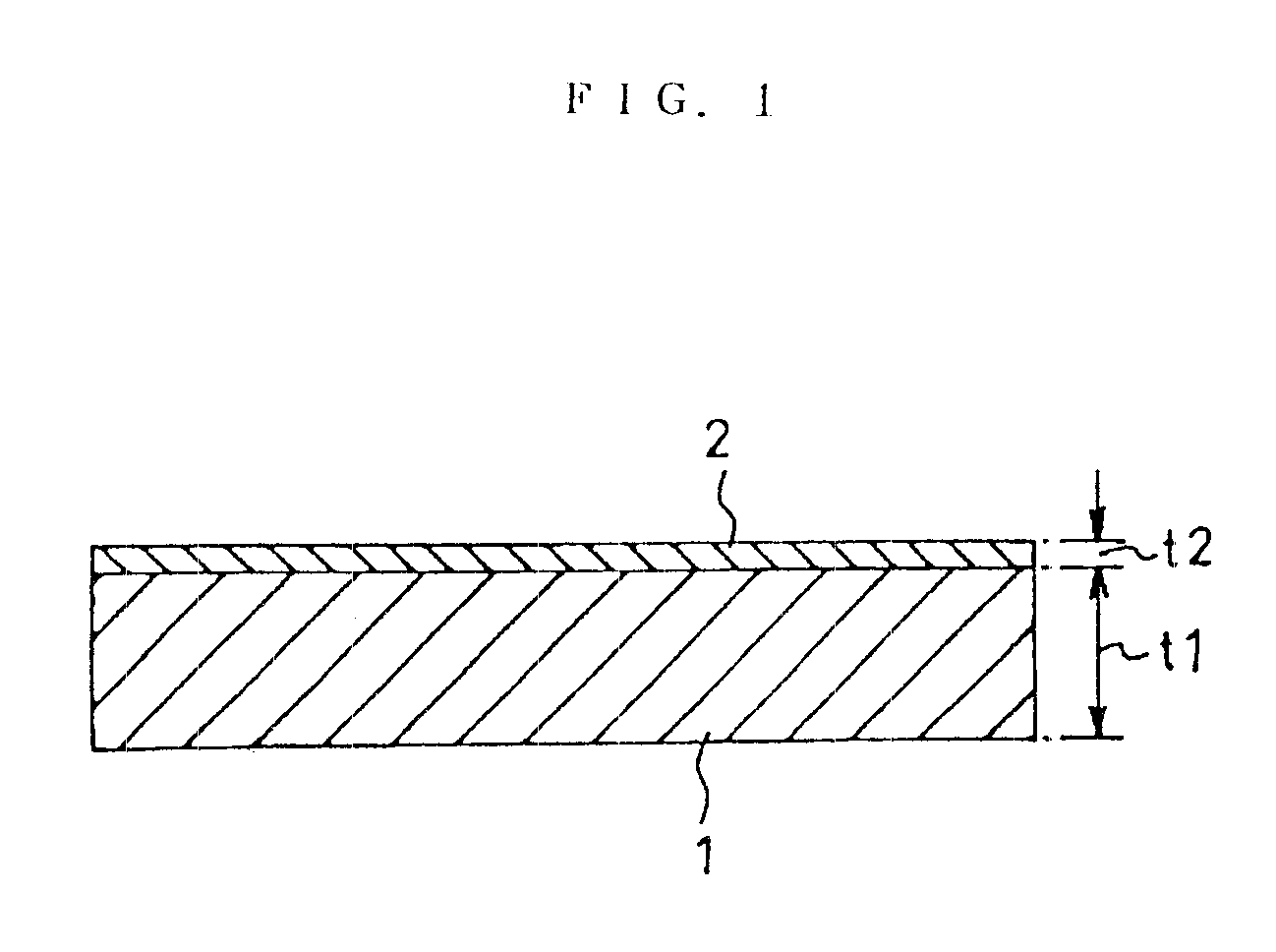
FIGS. 1 to 4 are views illustrating the results of steps of the method of producing such a single crystal SiC composite material for producing a semiconductor device of the invention. In a first step, the results of which are shown in FIG. 1, a single crystal SiC film 2 in which the thickness t2 is about 1 .mu.m is formed by the heteroepitaxial growth method on a single crystal Si substrate 1 in which the thickness t1 is about 0.5 cm.

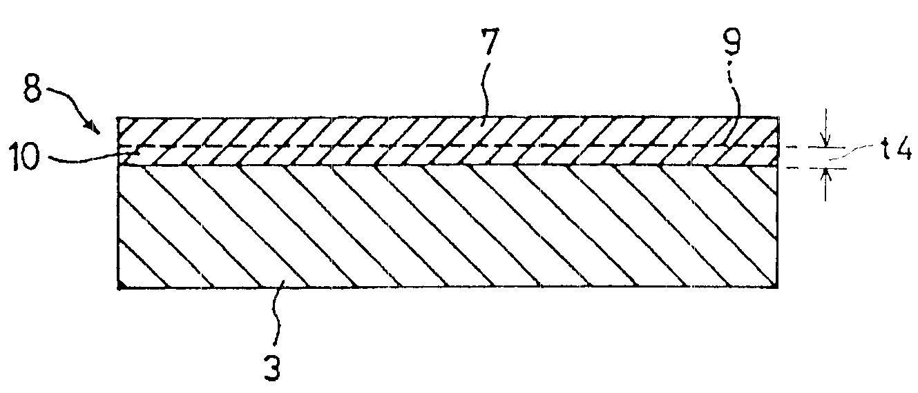
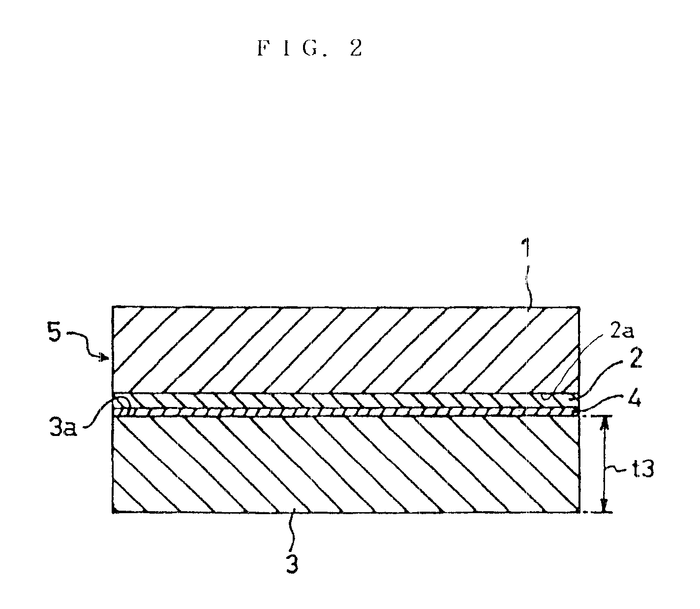
In a second step, the results of which are shown in FIG. 2, the single crystal SiC film 2 which is formed on the Si substrate 1 is then stacked via a film-like SiO.sub.2 layer 4 in a closely contacted manner onto a mirror-polished surface 3a of a polycrystalline plate 3 which is formed by the thermal CVD method into a flat plate-like shape having a thickness t3 of about 0.7 cm. As the SiO.sub.2 layer 4, any one of a member which is formed by applying SiO.sub.2 p...


PUM


Abstract

In a single crystal SiC composite material for producing a semiconductor device, and a method of producing the same according to the invention, a single crystal SiC film which is produced on an Si substrate by the heteroepitaxial growth method and obtained by removing the Si substrate, is stacked and bonded via a film-like SiO2 layer onto the surface of a polycrystalline plate consisting of Si and C atoms in a closely contacted manner forming thereby a stacked composite member. The stacked composite member is then heat-treated, whereby single crystal SiC in which the crystal is transformed in the same orientation as the single crystal of the single crystal SiC film is integrally grown on the polycrystalline plate. The thickness and the strength which are requested for producing a semiconductor device can be ensured, and lattice defects and micropipe defects seldom occur, so that an accurate and high-quality semiconductor device can be produced.

Description

1. Field of the InventionThe present invention relates to a single crystal SiC composite material for producing a semiconductor device, and a method of producing the same, and more particularly to a single crystal SiC composite material for producing, for example, a high-temperature or high-frequency device, or a radiation resistant device such as a light-emitting diode, an X-ray optical element, a switching element, an amplifying element, or an optical sensor, and also to a method of producing such a single crystal SiC composite material.2. Description of the Prior ArtSiC (silicon carbide) is superior in heat resistance and mechanical strength, and has good resistance to radiation. In addition, it is easy to perform the valence control of electrons and holes by doping an impurity. Moreover, SiC has a wide band gap (for example, single crystal 6H-SiC has a band gap of about 3.0 eV, and single crystal 4H-SiC has a band gap of 3.26 eV). Therefore, it is possible to realize a high-temp...

Claims


Application Information

Patent Timeline
IPC IPC(8): C30B25/02H01L21/02H01L21/04H01L21/324C30B29/36H01L21/203
CPCC30B25/02H01L21/0445C30B29/36H01L21/02002
Inventor TANINO, KICHIYAMUNETOMO, NOBUHIRO
Owner NISSIN ELECTRIC CO LTD
Why Eureka
Try Eureka