Surface structure and method of making, and electrostatic wafer clamp incorporating surface structure

a surface structure and electrostatic technology, applied in electrostatic charges, capacitors, electrical devices, etc., can solve the problems of uncontrollable diffusion of impurities beyond the described limits of the wafer, inability to meet the requirements of the substrate, and degradation of the patterned photoresist layer, etc., to achieve good structural integrity, efficient thermal transfer, and good shear strength

Inactive Publication Date: 2005-01-04
VARIAN SEMICON EQUIP ASSOC INC
View PDF28 Cites 37 Cited by
  • Summary
  • Abstract
  • Description
  • Claims
  • Application Information

AI Technical Summary

Benefits of technology

The coating may comprise a ceramic or other inert inorganic material with good structural integrity and good shear strength, and the flexible layer may comprise a polymer layer. In one embodiment, the flexible layer is silicone rubber having a thickness in a range of about 5 to 10 micrometers, and the coating is silicon nitride, silicon carbonitride, silicon dioxide or carbon having a thickness in a range of ab...

Problems solved by technology

However, large amounts of heat are likely to be generated by the high current ion beam.
The heat can result in uncontrolled diffusion of impurities beyond described limits in the wafer and in degradation of patterned photoresist layers.
However, the requirement for rotating the wafer mounting site in order to provide centrifugal clamping adds complexity and is not always practical.
Regardless of the clamping technique utilized, thermal transfer from a semiconductor wafer to a heat sink in vacuum is problematic.
Heat transfer by radiation from the wafer is inadequate, except for low current ion beams.
Even where the wafer is in physical contact with the platen surface, surface irregularities on the wafer and the platen surface limit actual contact to about 5% of the two surface areas and thereby limit solid-to-solid thermal conduction.
A disadvantage is that such materials are not inherently heat conductive.
The doping method has the disadvantage of adding an extra process step and the possibility of particle or elemental contamination by the heat conductive particles.
The increased pressure method has the disadvantage that the increased pressure may induce wafer break...

Method used


Image

  • Surface structure and method of making, and electrostatic wafer clamp incorporating surface structure
  • Surface structure and method of making, and electrostatic wafer clamp incorporating surface structure
  • Surface structure and method of making, and electrostatic wafer clamp incorporating surface structure

Examples


second embodiment

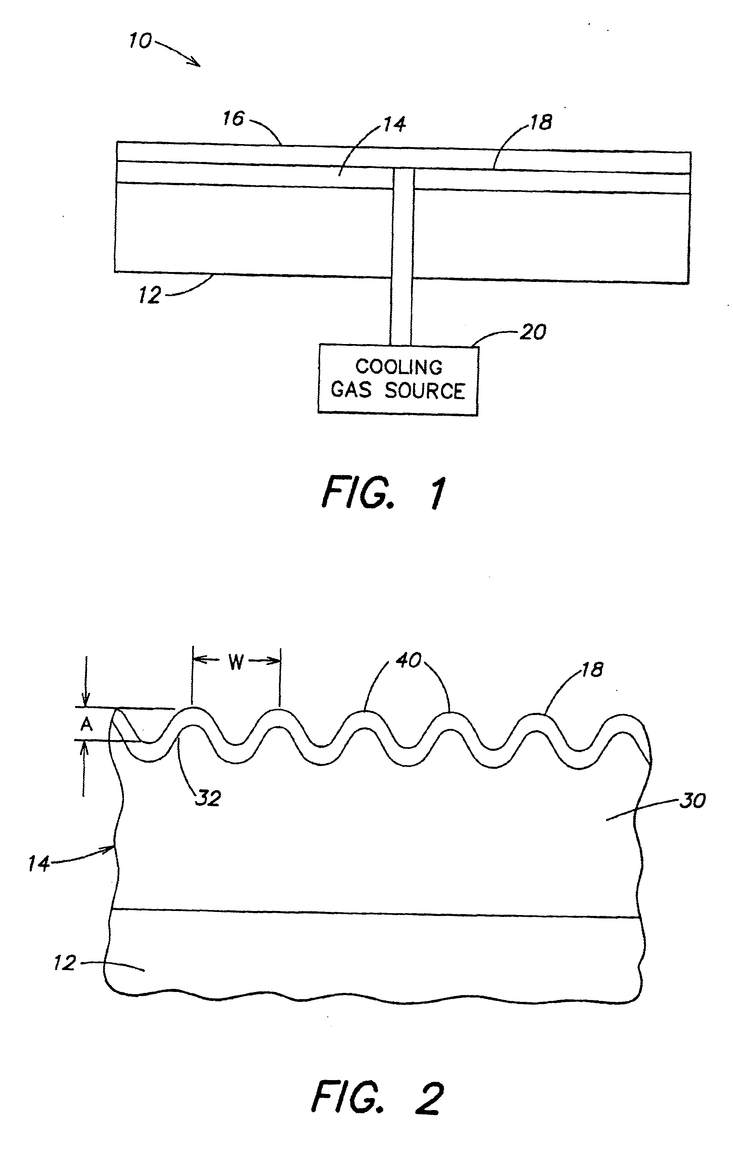
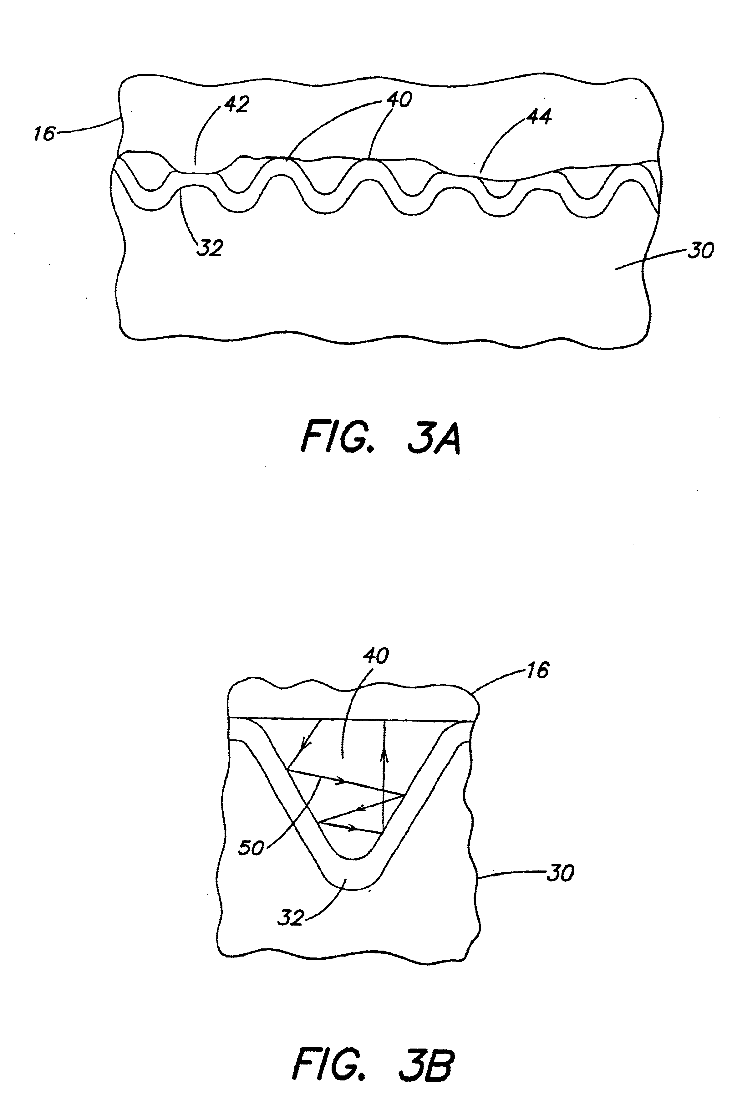
a surface structure is shown in FIG. 5. The surface structure provides low particle generation low particulate contamination of a workpiece, is resistant to molecular contamination and can be made to have either conducting or insulating electrical properties as needed. The surface has low abrasion properties and is therefore unlikely to cause damage, even on a microscopic scale, to a workpiece. The surface is resistant to external contamination and is relatively durable, and may be cleaned if necessary.

A surface structure 90 includes a workpiece support element 100, which may be made of any material. Examples include electrical and thermal conductors, such as aluminum, and electrical insulators, such as alumina. The surface structure 90 further includes an optional adhesive interface layer 102, a resilient, flexible layer 104 and a coating 106. The support element 100 must be chemically compatible with flexible layer 104 if flexible layer 104 is applied directly to support element 1...


PUM


Abstract

A surface structure for contacting a workpiece includes a flexible layer adhered to a support element and a coating on the flexible layer. The coating has ripples on its surface. The flexible layer may be thermally conductive. The ripples on the surface enhance thermal transfer from the workpiece and are characterized by low particle generation and low particulate contamination of the workpiece. The ripples in the coating may be formed by expanding the flexible layer, applying the coating to the expanded flexible layer and then contracting the flexible layer. In one application, the surface structure is utilized in an electrostatic wafer clamp. The surface structure provides high efficiency thermal transfer in a vacuum processing system when utilized in conjunction with a low pressure cooling gas between the workpiece and the surface structure.

Description

FIELD OF THE INVENTIONThis invention relates to surface structures for contacting a workpiece and to methods for making the surface structures and, more particularly, to surface structures for contacting semiconductor wafers in a vacuum processing chamber. The surface structures are characterized by highly efficient thermal transfer and low particulate contamination. The surface structures are particularly useful in electrostatic wafer clamps used in ion implantation systems, but are not limited to such use.BACKGROUND OF THE INVENTIONIn the fabrication of integrated circuits, a number of well established processes involve the application of ion beams to semiconductor wafers in vacuum. These processes include, for example, ion implantation, ion beam milling and reactive ion etching. In each instance, a beam of ions is generated in a source and is accelerated toward a target wafer.Ion implantation has become a standard technique for introducing dopant materials into semiconductor wafe...

Claims


Application Information

Patent Timeline
IPC IPC(8): H01L21/00H01L21/683H01L21/67
CPCH01L21/6831H01L21/67103
Inventor LARSEN, GRANT KENJI
Owner VARIAN SEMICON EQUIP ASSOC INC
Why Eureka
Try Eureka