

Method of fabricating semiconductor device
a semiconductor and field effect technology, applied in the direction of crystal growth process, polycrystalline material growth, chemistry apparatus and processes, etc., can solve the problems of twin plane, stacking fault, and inability to form a crystalline semiconductor film by specifying the position and size of crystal grains, so as to improve the cleanliness of air and prevent contaminant.
- Summary
- Abstract
- Description
- Claims
- Application Information
AI Technical Summary
Benefits of technology
Problems solved by technology
Method used
Image

Examples
example 1
[0270]This example is described on a crystalline semiconductor film formed by the art of the embodiment 3 by referring to FIGS. 18A and 18B. FIG. 18A shows an SEM photograph obtained by observing a secoetched state of a crystalline semiconductor film according to this embodiment from the upper side and FIG. 18B shows a schematic view of the crystalline semiconductor film.
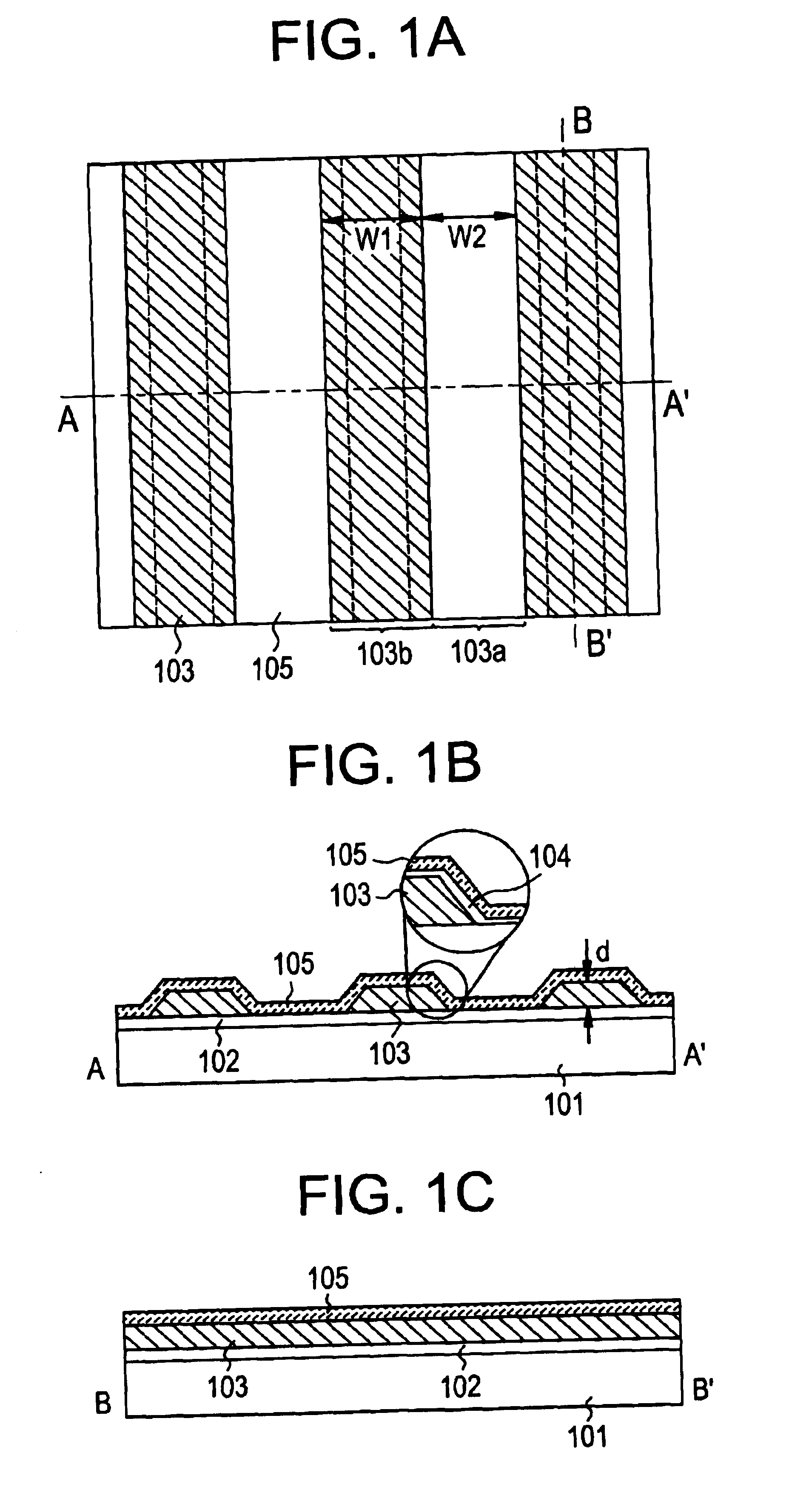
[0271]As conditions of this embodiment, a silicon nitride oxide film with a thickness of 50 nm is used as a first insulating film and a silicon oxide nitride film with a thickness of 200 nm is used as a second insulating film. In this case, the width (W1) of the second insulating film is set to 2 μm and the width (W2) between second insulating films is also set to 2 μm. Moreover, a silicon oxide nitride film with a thickness of 20 nm is formed on the second insulating film as a third insulating film and then, an amorphous silicon film with a thickness of 150 nm is continuously formed as an amorphous semiconductor fi...
example 2
[0273]For this example, a case is described in which all island-shaped semiconductor films are present only on concave portions.
[0274]First, up to the state shown in FIGS. 20A and 20B of the embodiment is formed.
[0275]Then, the entire surface of the semiconductor film 703 is etched to expose the upper face of the convex portion 701a of the ground film 701. According to the above step, a semiconductor film present only on a concave portion of the ground film 701 is formed. For removal from the upper face of the semiconductor film 703, it is allowed to use any method such as etching or CMP method.
[0276]According to the removal from the upper face, a portion at which a grain boundary is present on the convex portion 701a is removed and a semiconductor film having a high crystallinity which will serve as a channel-forming region later is left on a concave portion between the convex portions 701a.
[0277]Then, as shown in FIG. 25A, an island-shaped semiconductor film 772 serving as an act...
example 3
[0281]A method of forming a base film having unevenness is explained in Example 3. Incidentally, the base film described in this example is only one example and the base film used in the present invention is not limited to this.
[0282]A first base film 251 made form an insulating film is first formed on a substrate 250 as shown in FIG. 27A. The first base film 251 uses silicon oxynitride in this example but is not limited to this material, and insulating films having a large selectivity in etching with a second base film may be used. The first base film 251 is formed by a CVD apparatus using SiH4 and N2O so that its thickness is from 50 to 200 nm. Note that the first base film may be a single layer, and may also be a laminate structure of a plurality of insulating films.
[0283]A second base film 252 is formed next from an insulating material that contacts the first base film 251, as shown in FIG. 27B. It is necessary that the film thickness of the second base film 252 be of an order s...
PUM
 Abstract
Description
Claims
Application Information