High-speed silicon-based electro-optic modulator

a modulator and silicon-based technology, applied in the field of silicon-based electrooptic modulators, can solve the problems of reducing the effectiveness of the modulator, reducing the efficiency of the modulator, and slow thermal effect, so as to reduce the optical loss, reduce the series resistance, and reduce the effect of optical loss

Active Publication Date: 2005-01-18
CISCO TECH INC
View PDF24 Cites 193 Cited by
  • Summary
  • Abstract
  • Description
  • Claims
  • Application Information

AI Technical Summary

Benefits of technology

It is an advantage of the present invention that the doping of the silicon layers can be controlled to provide for lightly doped regions in the active free carrier movement region and more heavily doped regions in the contact area. Thus, the series resistance is minimized while also providing lower optical loss. The series resistance can be further reduced by adding a second contact for both the gate and body regions. Moreover, the inventive SISCAP design allows for the free carrier distribution to substantially overlap with the peak (or near peak) optical electric field, accumulating, depleting or inverting carriers on each side of the gate dielectric at the same time. Advantageously, both the lateral and vertical doping profiles can be controlled by CMOS processing to provide these and other device attributes. For example, lateral doping variations in the body and gate regions can be performed by using multiple mask definitions and implants. The vertical doping profile in the gate and body regions can be controlled (in one form, graded) through a single, dynamically-controlled implant process, multiple implants of different dopant concentrations and / or implant energies, and / or a multi-layer silicon deposition, each layer having a different dopant concentration.
that the doping of the silicon layers can be controlled to provide for lightly doped regions in the active free carrier movement region and more heavily doped regions in the contact area. Thus, the series resistance is minimized while also providing lower optical loss. The series resistance can be further reduced by adding a second contact for both the gate and body regions. Moreover, the inventive SISCAP design allows for the free carrier distribution to substantially overlap with the peak (or near peak) optical electric field, accumulating, depleting or inverting carriers on each side of the gate dielectric at the same time. Advantageously, both the lateral and vertical doping profiles can be controlled by CMOS processing to provide these and other device attributes. For example, lateral doping variations in the body and gate regions can be performed by using multiple mask definitions and implants. The vertical doping profile in the gate and body regions can be controlled (in one form, graded) through a single, dynamically-controlled implant process, multiple implants of different dopant concentrations and / or implant energies, and / or a multi-layer silicon deposition, each layer having a different dopant concentration.
In accordance with the present invention, conventional CMOS processing and device elements are used to form an electro-optic modulator with sub-micron dimensions. Since the modulator is based on a capacitive structure, it draws no power in a static mode (that is, no power is required to maintain a logic state), thus exhibiting a significant reduction in power consumption when compared to prior art device arrangements.
There exist various SISCAP configurations, as well as doping arrangements, polysilicon grain size enhancements and grain boundary passivation techniques that may be used to provide the sub-micron electro-optic modulator of the present invention. It is expected that the present invention will take advantage of advances made in the state-of-the-art CMOS processing field. For example, the teachings of the present invention are compatible with alternative dielectric gate materials, such as materials used for nanometer-scale CMOS devices.

Problems solved by technology

Nevertheless, the thermo-optic effect is rather slow and can only be used for device speeds up to 1 Mb / s modulation frequency.
Long interaction lengths are undesirable in order to achieve high levels of integration and miniaturization for fabricating low-cost compact device arrangements.
High current densities may induce unwanted thermo-optic effects as a result of heating the structure and will, indeed, cause an opposite effect on the real refractive index change relative to that associated with free carrier movement, thus reducing its effectiveness.
However, to act as an optical modulator, the speed of operation of electro-optic modulator 1 is limited by the lifetime of free carriers in rib 3, as well as the carrier diffusion rates when the forward bias is removed.
By introducing impurities into the silicon, which act as carrier lifetime “killers”, the switching speed can be increased, but the introduced impurities detrimentally affect the optical transmission.
Theoretically, high speed operation of a PN junction could be achieved in reverse bias, although this would require large drive voltages and long device lengths, which are incompatible with the CMOS process.

Method used


Image

  • High-speed silicon-based electro-optic modulator
  • High-speed silicon-based electro-optic modulator
  • High-speed silicon-based electro-optic modulator

Examples


first embodiment

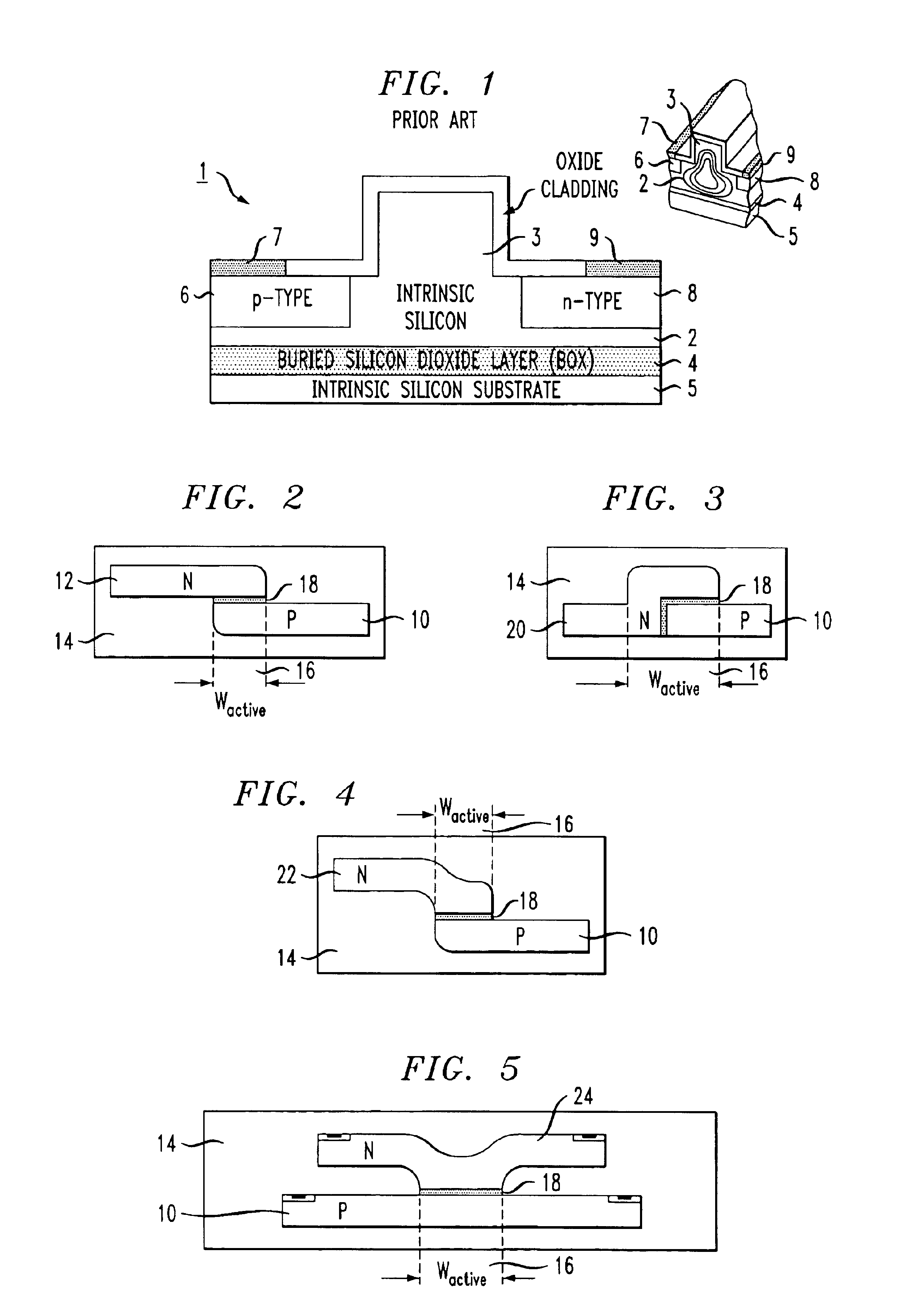
With this basic understanding of various aspects of the present invention, FIG. 8 illustrates an electro-optic modulator device 30 formed in accordance with the present invention. It is to be understood that there exist various processing techniques that may be used to form the device as shown. The present invention is directed to the utilization of the unique overlap of the optical electric field and free carrier areas by virtue of the SISCAP structure exhibiting inherent, effective index guiding. Accordingly, the inventive structure may be formed using any acceptable process sequence that yields the various device elements, element positions and associated doping levels required for acceptable operation. In each case, the basis of the present invention is the utilization of an SOI wafer, incorporating the modulator elements within and above the relatively thin, sub-micron surface silicon layer to form a SISCAP structure, while also advantageously utilizing the buried oxide (or die...

second embodiment

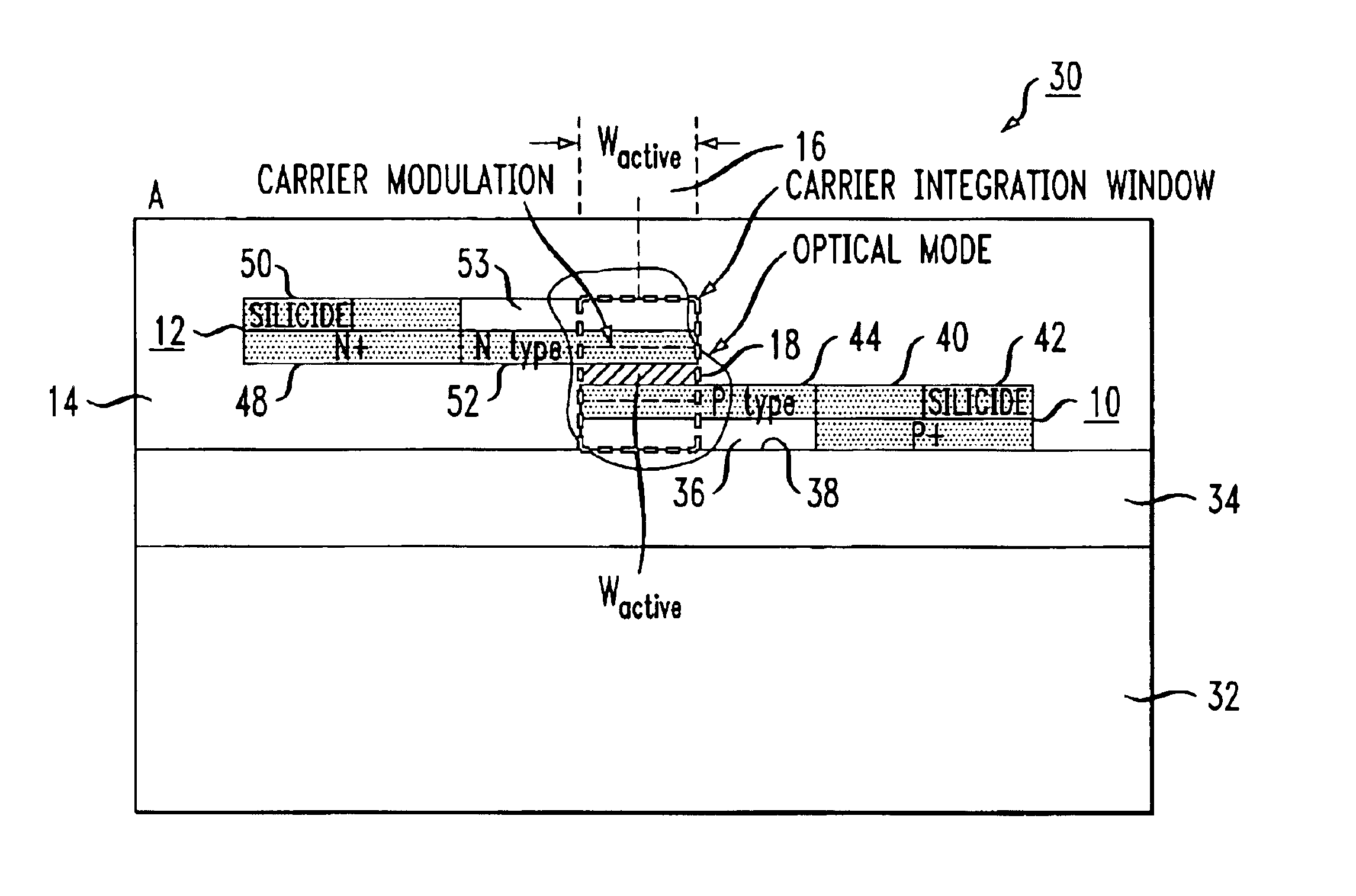
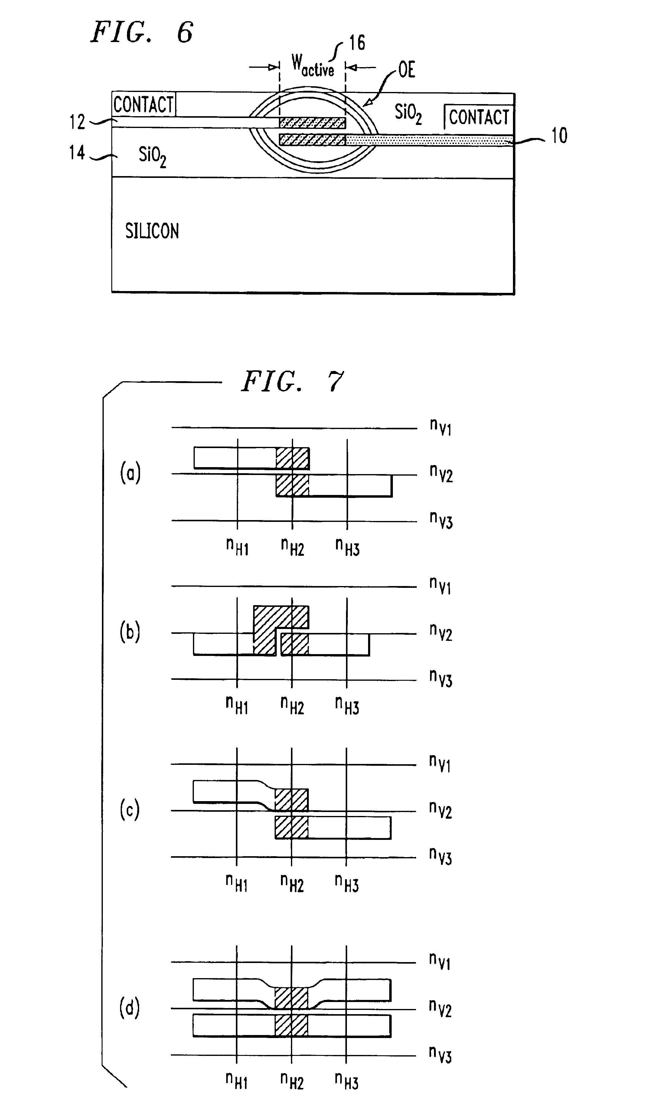
FIG. 13 illustrates an electro-optic modulator formed in accordance with the present invention. Electro-optic modulator 60 as shown in FIG. 13 utilizes the gate region geometry as discussed above in association with FIG. 3. In particular, modulator 60 comprises relatively thin n-type gate region 20 and relatively thin p-type body region 10, where p-type region 10 is formed by implanting a dopant such as boron to form regions 36, 40 and 44. Region 42 is preferably a silicide, such as tantalum, cobalt, nickel, molybdenum, tungsten or titanium silicide. After appropriately etching region 10, the gate dielectric 18 is formed and region 20 is deposited in one or multiple layers using implantation of a dopant such as phosphorous, arsenic or antimony to form portions 48, 52 and 53. As with contact 42, contact 50 is also preferably formed from a silicide. Similar to modulator 30 of FIG. 8, modulator 60 of FIG. 13 includes portions 36 and 53 that are more lightly doped (or even undoped) than...


PUM

PropertyMeasurementUnit
thicknessaaaaaaaaaa
voltageaaaaaaaaaa
lengthaaaaaaaaaa

Abstract

A silicon-based electro-optic modulator is based on forming a gate region of a first conductivity to partially overly a body region of a second conductivity type, with a relatively thin dielectric layer interposed between the contiguous portions of the gate and body regions. The modulator may be formed on an SOI platform, with the body region formed in the relatively thin silicon surface layer of the SOI structure and the gate region formed of a relatively thin silicon layer overlying the SOI structure. The doping in the gate and body regions is controlled to form lightly doped regions above and below the dielectric, thus defining the active region of the device. Advantageously, the optical electric field essentially coincides with the free carrier concentration area in this active device region. The application of a modulation signal thus causes the simultaneous accumulation, depletion or inversion of free carriers on both sides of the dielectric at the same time, resulting in high speed operation.

Description

TECHNICAL FIELDThe present invention relates to a silicon-based electro-optic modulator and, more particularly, to an electro-optic modulator based on SOI technology and utilizing a Silicon-Insulator-Silicon CAPacitor (SISCAP) guide geometry to provide efficient, high-speed operation.BACKGROUND OF THE INVENTIONSilicon-based photonic components working at 1330 and 1500 nm fiber-optic communication wavelengths for various systems such as fiber-to-the-home and local area networks (LANs) are a subject of intensive research as a result of the possibility of integrating optical elements and advanced electronics together on a silicon substrate using the well-known techniques of CMOS technology.Passive silicon structures, such as waveguides, couplers and filters have been extensively studied. Less work has been reported on active silicon devices (i.e., tunable devices), such as modulators and switches, despite their importance as a means of manipulating light beams for such communication sy...

Claims


Application Information

Patent Timeline
Patent Type & Authority Patents(United States)
IPC IPC(8): G02F1/025G02F1/01G02F1/225
CPCG02F1/2257G02F1/025G02B2006/12142G02B2006/12159
Inventor MONTGOMERY, ROBERT KEITHGHIRON, MARGARETGOTHOSKAR, PRAKASHPATEL, VIPULKUMARSHASTRI, KALPENDUPATHAK, SOHAMYANUSHEFSKI, KATHERINE A.
Owner CISCO TECH INC
Why Eureka
Try Eureka