Polymeric antireflective coatings deposited by plasma enhanced chemical vapor deposition

a technology antireflective coatings, which is applied in the direction of chemical vapor deposition coatings, resistive material coatings, metallic material coating processes, etc., can solve the problems of insufficient planarization, limited performance, and magnified inherent inefficiencies of spin coating processes, so as to minimize negative effects, reduce overall waste, and minimize was

Inactive Publication Date: 2005-02-08
BREWER SCI
View PDF3 Cites 15 Cited by
  • Summary
  • Abstract
  • Description
  • Claims
  • Application Information

AI Technical Summary

Benefits of technology

Finally, in addition to the aforementioned antireflective layer properties, the instant invention has a further distinct advantage over prior art spincoating methods which utilize large quantities of solvents. That is, the instant methods avoid spincoating solvents which often require special handling. Thus, solvent waste is minimized and so are the negative effects that solvent waste can have on the environment. Furthermore, overall waste is minimized with the inventive process wherein substantially all of the reactants are consumed in the process.

Problems solved by technology

While spincoated antireflective layers offer excellent reflectivity control, their performance is limited by their nonuniformity, defectivity and conformality constrictions, and other inefficiencies inherent within the spincoating process.
As the industry approaches the adoption of eight-inch or even twelve-inch semiconductor substrates, the inherent inefficiencies of the spincoating process become magnified.
Although high optical densities at DUV wavelengths enable these pre-designed polymers to provide effective reflectivity control at prior art dimensions, they have numerous drawbacks.
One problem with the currently available antireflective coating application processes is inadequate planarization.
The formed layers typically lack uniformity in that the thickness at the edge of the substrate is greater than the thickness at the center.
Furthermore, spincoated antireflective coating layers tend to planarize or unevenly coat surface topography rather than form highly conformal layers (i.e., layers which evenly coat each aspect of the substrate and the features).
That is, in the process of clearing the antireflective coating from the troughs by plasma etch, the sidewalls of the resist features become eroded, producing microscopically-sized—but significant—changes in the feature shape and / or dimensions.
Furthermore, the resist thickness and edge acuity may be lost, which can lead to inconsistent images or feature patterns as the resist pattern is transferred into the substrate during subsequent etching procedures.
Other problems can occur as well due to the fact that spincoating of these ultra-thin antireflective coating layers takes place at very high speeds in a dynamic environment.
Accordingly, pinholes, voids, striations, bubbles, localized poor adhesion, center-to-edge thickness variations, and other defects occur as a consequence of attendant rapid or non-uniform solvent evaporation, dynamic surface tension, and liquid-wavefront interaction with the surface topography.

Method used


Image

  • Polymeric antireflective coatings deposited by plasma enhanced chemical vapor deposition
  • Polymeric antireflective coatings deposited by plasma enhanced chemical vapor deposition
  • Polymeric antireflective coatings deposited by plasma enhanced chemical vapor deposition

Examples


examples

The following examples set forth preferred methods in accordance with the invention. It is to be understood, however, that these examples are provided by way of illustration and nothing therein should be taken as a limitation upon the overall scope of the invention.

Materials and Methods

examples 1-3

The PECVD process to which the antireflective compounds were subjected in the following Examples 1-3 involved subjecting the compounds to sufficient electric current and pressure so as to cause the solid or liquid compounds to form a plasma. The monomers to be deposited were initially weighed in a glass vial (generally around 0.2 g although the amount consumed is not known). The vial containing the monomers was attached (via a rubber stopper) to a quartz chamber connected to a stainless steel pipe, with flow through the steel pipe being controlled by a needle valve. The quartz chamber was surrounded by an RF coil which, in turn, was connected to an RF generator. The RF generator generated the electric current in the quartz chamber through the RF coil. The quartz chamber was also connected to a deposition chamber in which the substrates were loaded.

The pressure of the system was increased to a level of from about 10-200 mTorr, more preferably from about 25-150 mTorr, and even more pr...

example 1

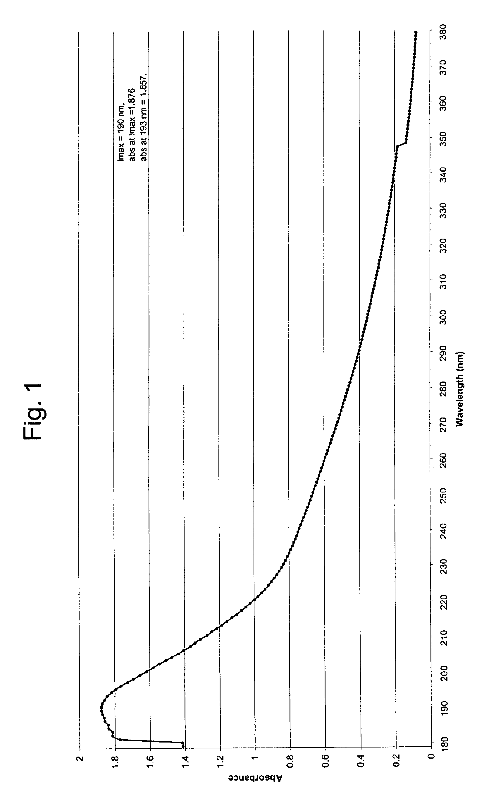
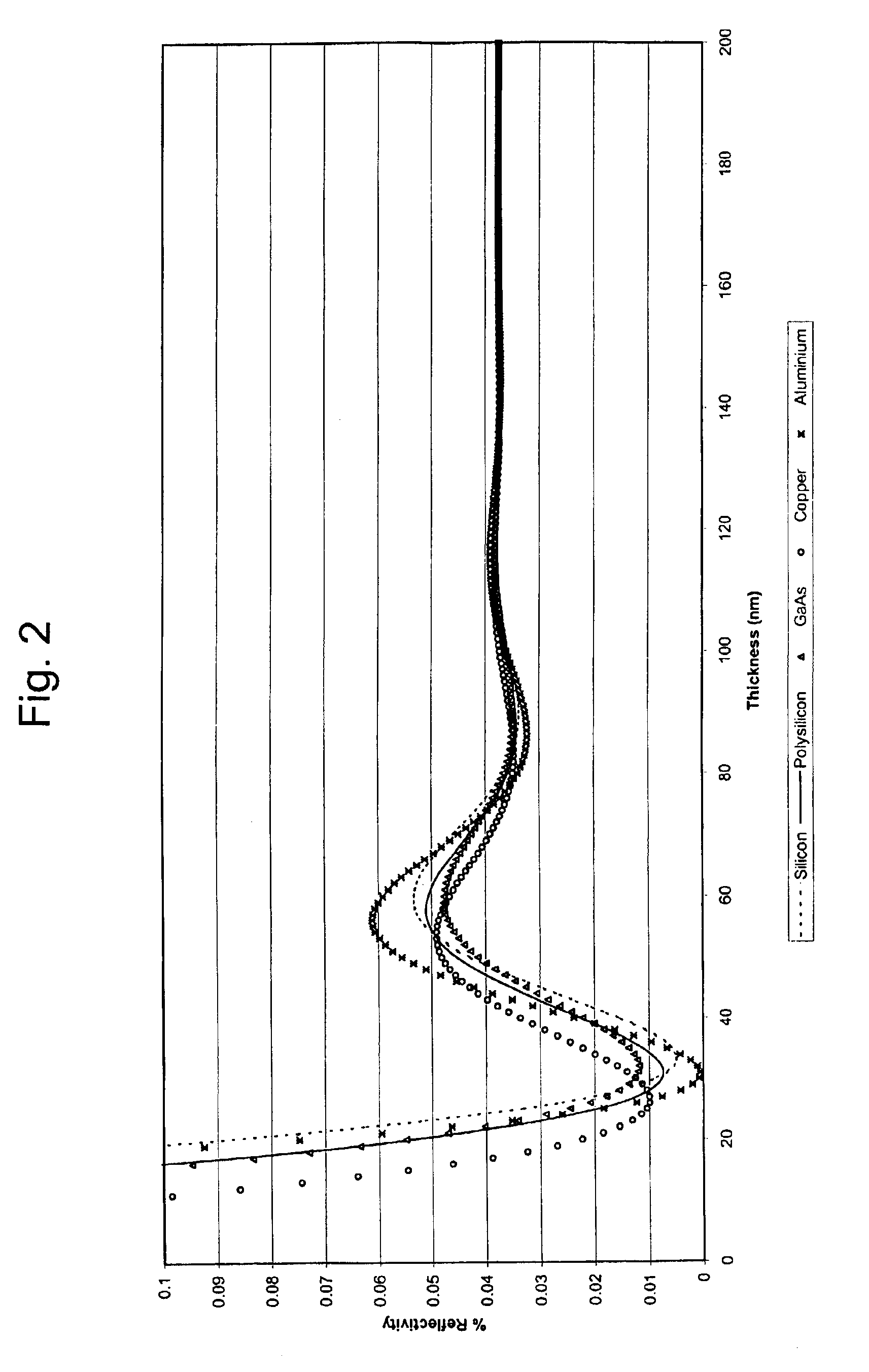
The deposition rate of phenylacetylene according to Example 1 was 200 Å / min., which is within the desired deposition range in the semiconductor industry standard for batch processing tools.

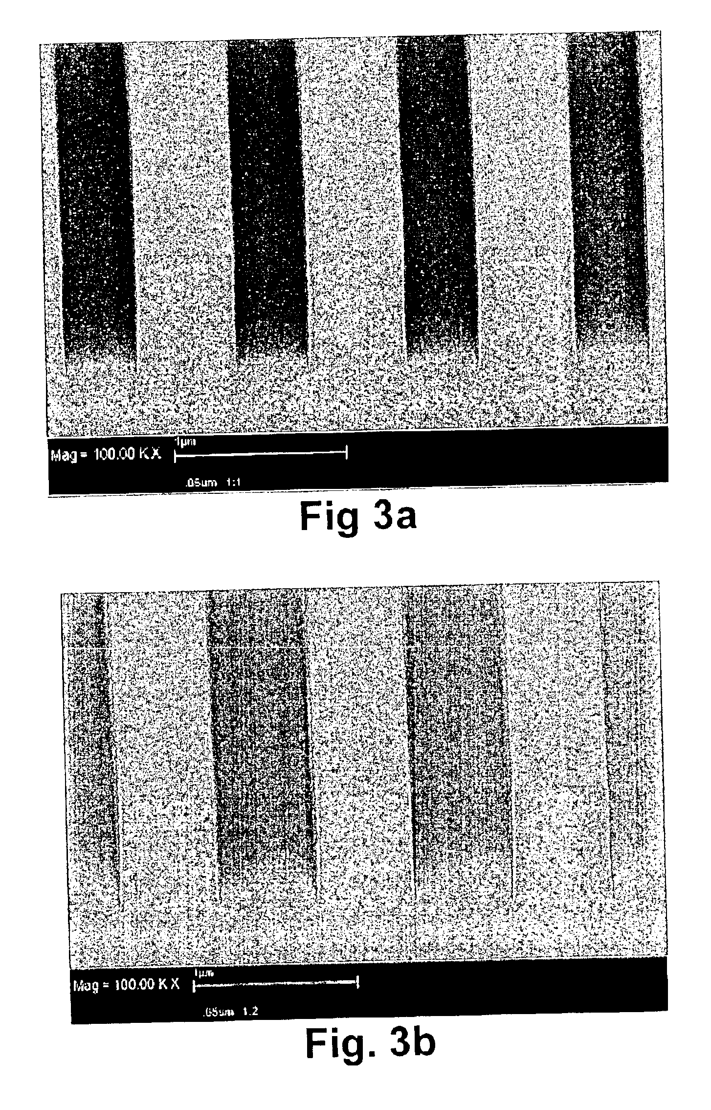
The film of phenylacetylene was deposited on silicon wafers, and the film thickness was optically measured by ellipsometry at 25 points on a planar silicon wafer to estimate the mean thickness. The phenylacetylene generated uniform coats, without pinholes, voids, or particles, having a preferred thickness of 400 Å. The films exhibited a thickness uniformity of >96% on 4-inch and 8-inch silicon wafers.

The solubility of phenylacetylene was examined by treating the film with solvents typically used in the semiconductor industry. The solvents evaluated were ethyl lactate and propylene glycol monomethyl ether acetate (PGMEA). Very little thickness loss was observed (see Table 2).

TABLE 2Stripping TestInitial Thick-Final Thick-StrippingSampleSolventness (Å)ness (Å)(%)phenylacetylenePGMEA9709620.8phenylac...


PUM

PropertyMeasurementUnit
boiling pointaaaaaaaaaa
pressureaaaaaaaaaa

Abstract

An improved method for applying polymeric antireflective coatings to substrate surfaces and the resulting precursor structures are provided. Broadly, the methods comprise plasma enhanced chemical vapor depositing (PECVD) a polymer on the substrate surfaces. The PECVD processes comprise providing a quantity of a polymer generated by introducing monomer vapors into a plasma state followed by polymerization thereof, with assistance of plasma energy, onto the surface of a substrate. The most preferred starting monomers are phenylacetylene, 4-ethynyltoluene, and 1-ethynyl-2-fluorobenzene. The inventive methods are useful for providing highly conformal antireflective coatings on large surface substrates having super submicron (0.25 μm or smaller) features. The process provides a much faster deposition rate than conventional chemical vapor deposition (CVD) methods, is environmentally friendly, and is economical.

Description

BACKGROUND OF THE INVENTION1. Field of InventionThe present invention is broadly concerned with methods of forming antireflective coating layers on silicon and dielectric materials as well as the resulting integrated circuit precursor structures. More particularly, the inventive methods comprise providing a quantity of a polymer generated by the introduction of monomers into a plasma state by electric current and subsequent polymerization thereof, with the aid of plasma energy, onto the surface of a substrate.2. Background of the Prior ArtIntegrated circuit manufacturers are consistently seeking to maximize silicon wafer sizes and minimize device feature dimensions in order to improve yield, reduce unit case, and increase on-chip computing power. Device feature sizes on silicon chips are now submicron in size with the advent of advanced deep ultraviolet (DUV) microlithographic processes. However, reducing the substrate reflectivity to less than 1% during photoresist exposure is crit...

Claims


Application Information

Patent Timeline
Patent Type & Authority Patents(United States)
IPC IPC(8): B05D7/24C09D165/00C09D4/00G03F7/09G03F7/16G03F7/11H01L21/027H01L21/312
CPCB05D1/62C09D4/00C09D165/00G03F7/091C08F238/00G02B1/111H01L21/0276G03F7/167G03F7/004
Inventor SABNIS, RAM W.
Owner BREWER SCI
Why Eureka
Try Eureka