Printing of electronic circuits and components

Inactive Publication Date: 2005-02-15
SRI INTERNATIONAL
View PDF22 Cites 100 Cited by
  • Summary
  • Abstract
  • Description
  • Claims
  • Application Information

AI Technical Summary

Benefits of technology

In another aspect, the solution being deposited preferably has a very low concentration of particulates, such as ≦5 wt % or ≦2 wt %. Especially preferred solutions have essentially no particulates, and are there

Problems solved by technology
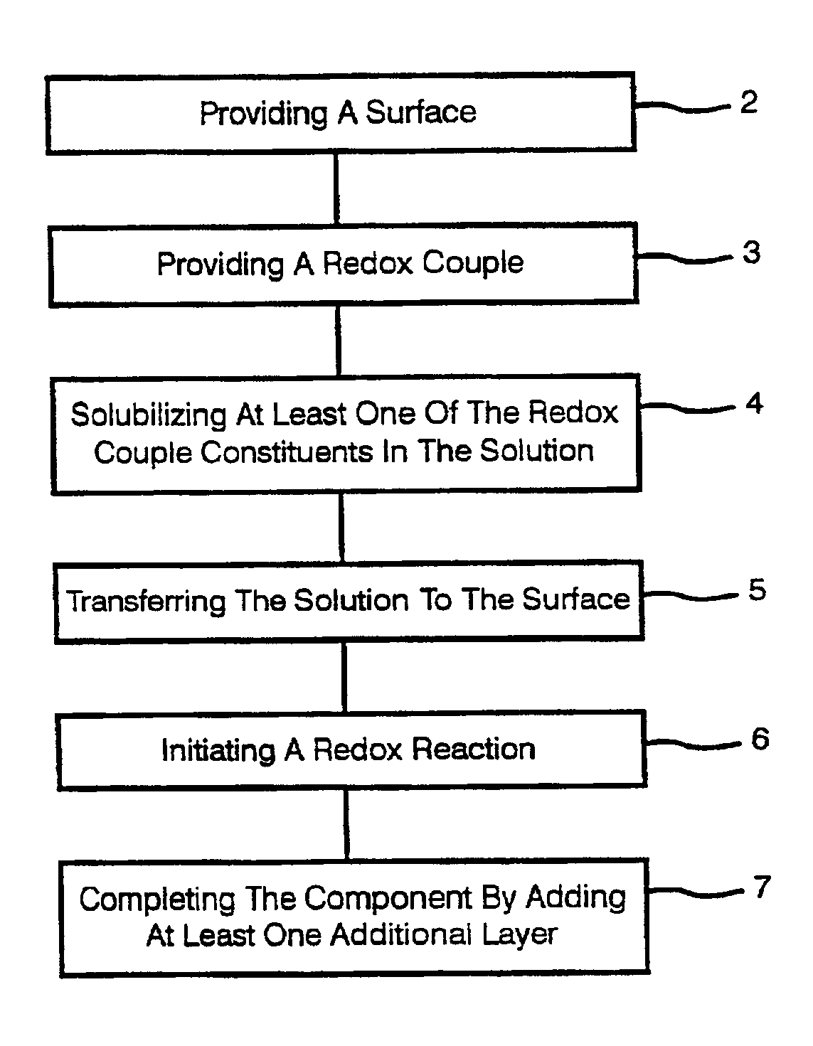
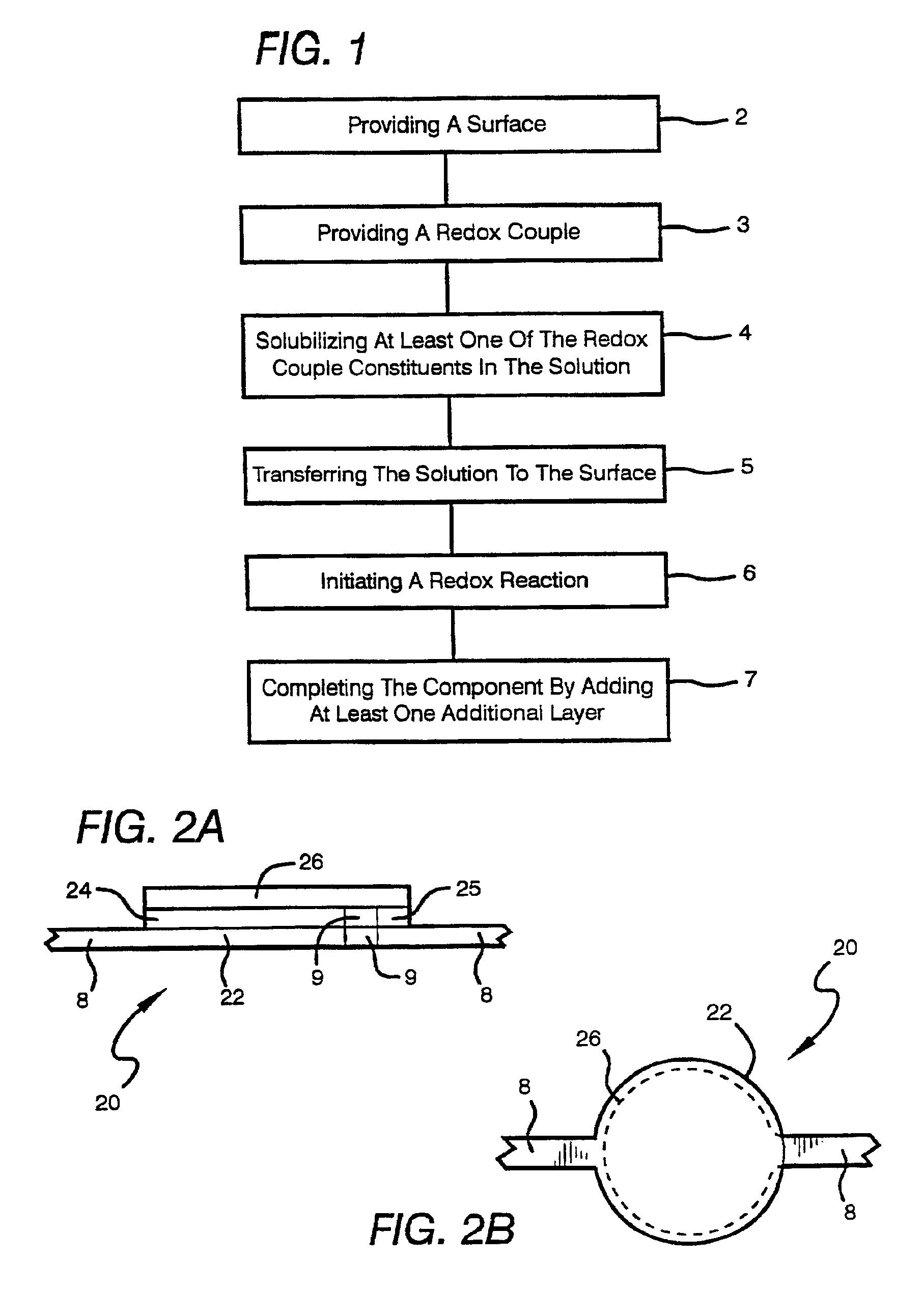
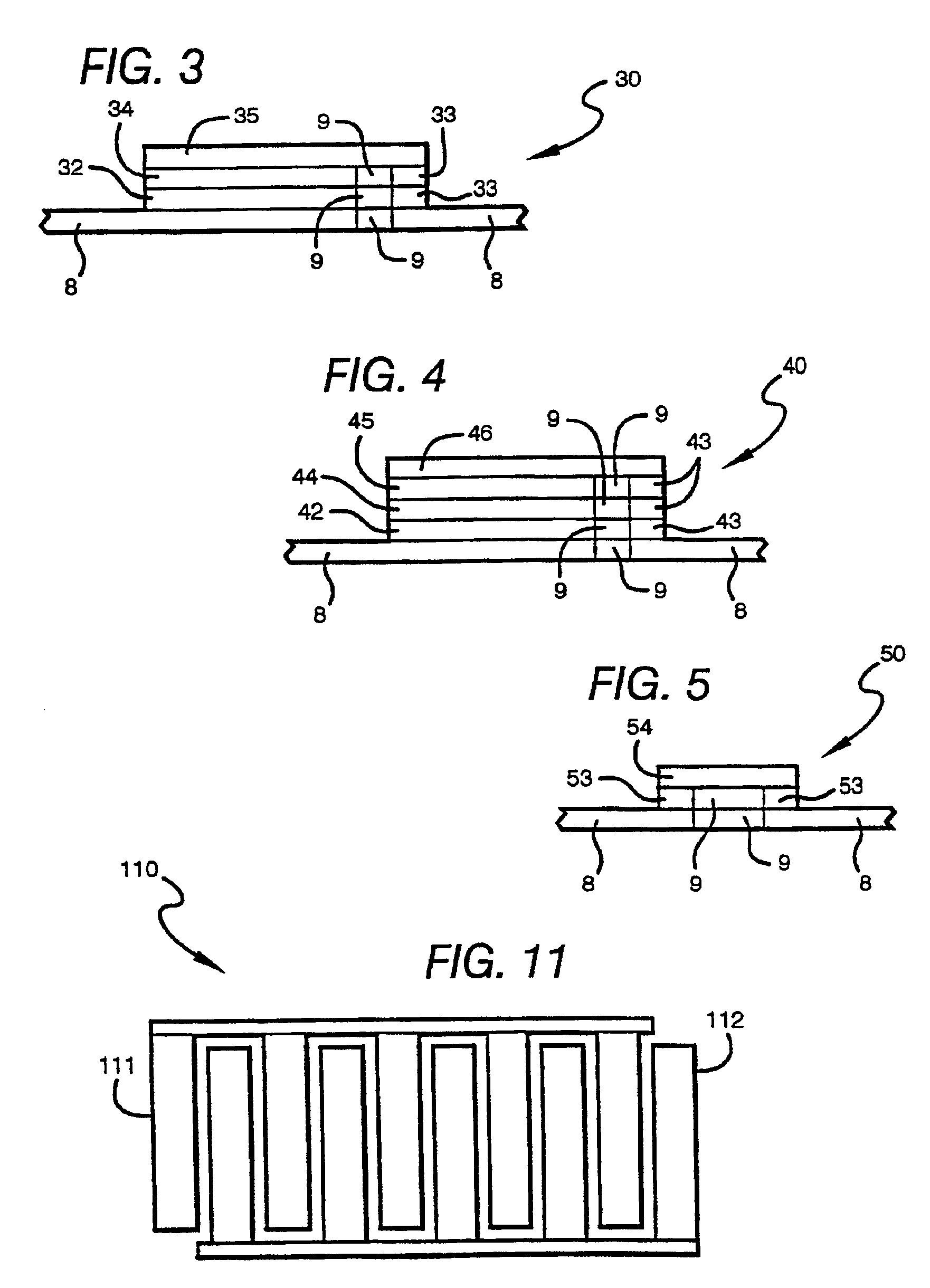
However, such devices are severely limited as to the type and complexity of the circuit and components, and there remains a considerable need for more versatile apparatus and techniques for printing circuits and components.
This situation results at least in part from production of circuit boards by processes that are incapable of providing the multiple layers needed for many electronic components.
While such techniques are capable of producing single layers of high quality and definition, they are not well suited for depositing multiple layers, especially multiple layers of different materials.
Especially inconsistent with standard circuit board printing techniques are printing of multilayer components such as batteries, which require specialized materials for the anode, cathode and electrolyte layers.
Other techniques commonly used to print circuit boards, such as silk screening, are capable of printing multiple layers, but they do not lend themselves to printing anything but the simplest electronic components.
In addition to forming relatively poor conductors, the particle size effectively limits the smallest trace to several times the diameter of the largest particles.
Still further, the potential for discontinuities in narrow traces and thin deposits appears to pose a problem of sufficient significance that repeated depositions, at slight offsets or angles are necessary to achieve reliable traces.
Another disadvantage is that Lowe is limited to printing electronic components that include only conductive, resistive and insulative portions.
Lowe also offers no guidance in the printing of semiconductors.
Even if known silk screening techniques were capable of printing the fineness required for electronic components, they would still be too slow for mass production of circuit/circuit component combinations.
Such impurities adversely affect conductivity and other function.
Another drawback is that

Method used


Image

  • Printing of electronic circuits and components
  • Printing of electronic circuits and components
  • Printing of electronic circuits and components

Examples


example 1

Copper Traces

Copper traces can be prepared by depositing a solution of copper (II) formate in conjunction with a nitrogen donor molecule. 2.0 g of copper (II) formate tetrahydrate was taken in a 100 ml round bottom flask and 6.8 g of cyclohexylamine was added to it. The mixture is stirred at room temperature (25-30° C.) for about 5 to 6 days to obtain a homogeneous viscous mass. Another 0.5 g of cyclohexylamine was added and stirring continued for another 24 hours, a thick paste was obtained. The viscosity of the solution was modified by adding an approximately 2 g of cyclohexylamine. The solution was dispensed using an ink-jet type printer in lines approximately 25 μm wide and 0.2 μm high. The deposited solution was then microwaved for 10 seconds, yielding substantially pure copper traces.

example 2

Insulators

4.5 g Kynar 721 PVDF is used to dissolve the binder in 5.6 g of NMP. The mixture is heated to 120° C. to ensure the PVDF dissolves fully. 97 g aluminum oxide powder was added. The slurry is mixed for 12 hours. The viscosity of the slurry is adjusted using NMP depending on the printing method.

example 3

Dielectrics

In a particular example barium titanate dielectric materials can be produced. 10 g of titanium (IV) isopropoxide in 30 ml of isopropyl alcohol in a 100 ml round bottom flask with a stirrer bar. In a 50 ml beaker 4 g of isobutyric and 5.5 g of acrylic acid dissolved in 20 ml of isopropyl alcohol. This solution of mixed acids was slowly added to the stirring solution of titanium (IV) isopropoxide prepared above. Stirring was continued for three hours at room temperature. A clear solution is obtained. 23.2 ml of the resulting solution was taken and added to a solution of 7 g of barium perchlorate was dissolved in about 80 ml of isopropyl alcohol. This mixture is allowed to stir for 1 hour to obtain a clear solution. This clear solution is printable.


PUM

PropertyMeasurementUnit
Lengthaaaaaaaaaa
Lengthaaaaaaaaaa
Lengthaaaaaaaaaa

Abstract

Methods are disclosed for printing (2-7) multilayer electronic components, and circuits on a surface (2), where at least one of the layers is formed by a redox reaction (6) occurring in a deposited solution (4, 5). Electronic components may comprise semiconductors such as in transistors or diode, or metal oxide or electrolyte such as in batteries or fuel cells, or are capacitors, inductors, and resistors. Preferably, the oxidizer of the redox reaction is a strong oxidizer, and the reducer is a strong reducer (3). Reactions are preferably sufficiently exothermic that they can be initiated (6), rather than driven to completion, by microwave or other suitable energy sources, and may yield substantially pure metal or metal oxide layers. The solution being deposited (5) may have either high concentrations of particulates, such as 60-80 wt. % of dry weight, or low concentrations of particulates, such as ≦5 wt. % or ≦2 wt. %. Low particulate content provides printing of structures having lateral resolution of ≦10 μm, ≦5 μm, or ≦1 μm.

Description

FIELD OF THE INVENTIONThe field of the invention is printing of electronic circuits and components.BACKGROUND OF THE INVENTIONElectronic circuits and components are ubiquitous in almost every field of the modern world, from communications to computing, transportation, energy production, storage and control, consumer goods, radios, navigation, and so forth. In each of these fields there continues to be a demand to produce ever smaller and less expensive products, and this demand in turn manifests as a push for ever more integrated circuits and components.The earliest electronic products were, of course, wired by hand. While some products are still produced at least in part by hand, hand produced circuit boards have largely been supplanted by machine printed circuit boards, and discrete components have largely been supplanted by highly integrated components such as LSICs and VLICs.Despite these advancements, most electronic devices are still generally manufactured by printing a circui...

Claims


Application Information

Patent Timeline
IPC IPC(8): C23C18/16H01M4/02H01M4/04H01M10/04H05K3/10H05K1/16H01M10/40H01M10/36H01M6/40H05K3/12H01C17/06H01F17/00H01G4/228H01G4/33H01L21/288H01L51/40H01M4/13H01M10/052
CPCH01G4/228C23C18/14H01M4/04H01M4/0402H01M4/0404H01M4/0414H01M4/0416H01M4/049H01M4/0492H01M4/13H01M10/0436H05K1/162H05K3/105C23C18/06C23C18/1216H01L21/288H01L51/0004H01M6/40H01M10/052H05K1/16H05K3/125H05K2203/013H05K2203/102H05K2203/1157H05K2203/1163Y02E60/122C23C18/143Y02E60/10Y02P70/50H10K71/13
Inventor NARANG, SUBHASH
Owner SRI INTERNATIONAL
Why Eureka
Try Eureka