

Semiconductor device and method of fabricating the same
a technology of semiconductor devices and semiconductor integrated circuits, which is applied in the direction of semiconductor devices, instruments, electrical equipment, etc., can solve the problems of tfts not having sufficient high reliability to be used in active-matrix devices, limiting the speed of prior-art semiconductor integrated circuits, and severely restricting their use, etc., to achieve optimal manufacturing process
- Summary
- Abstract
- Description
- Claims
- Application Information
AI Technical Summary
Benefits of technology
Problems solved by technology
Method used
Image

Examples
example 2
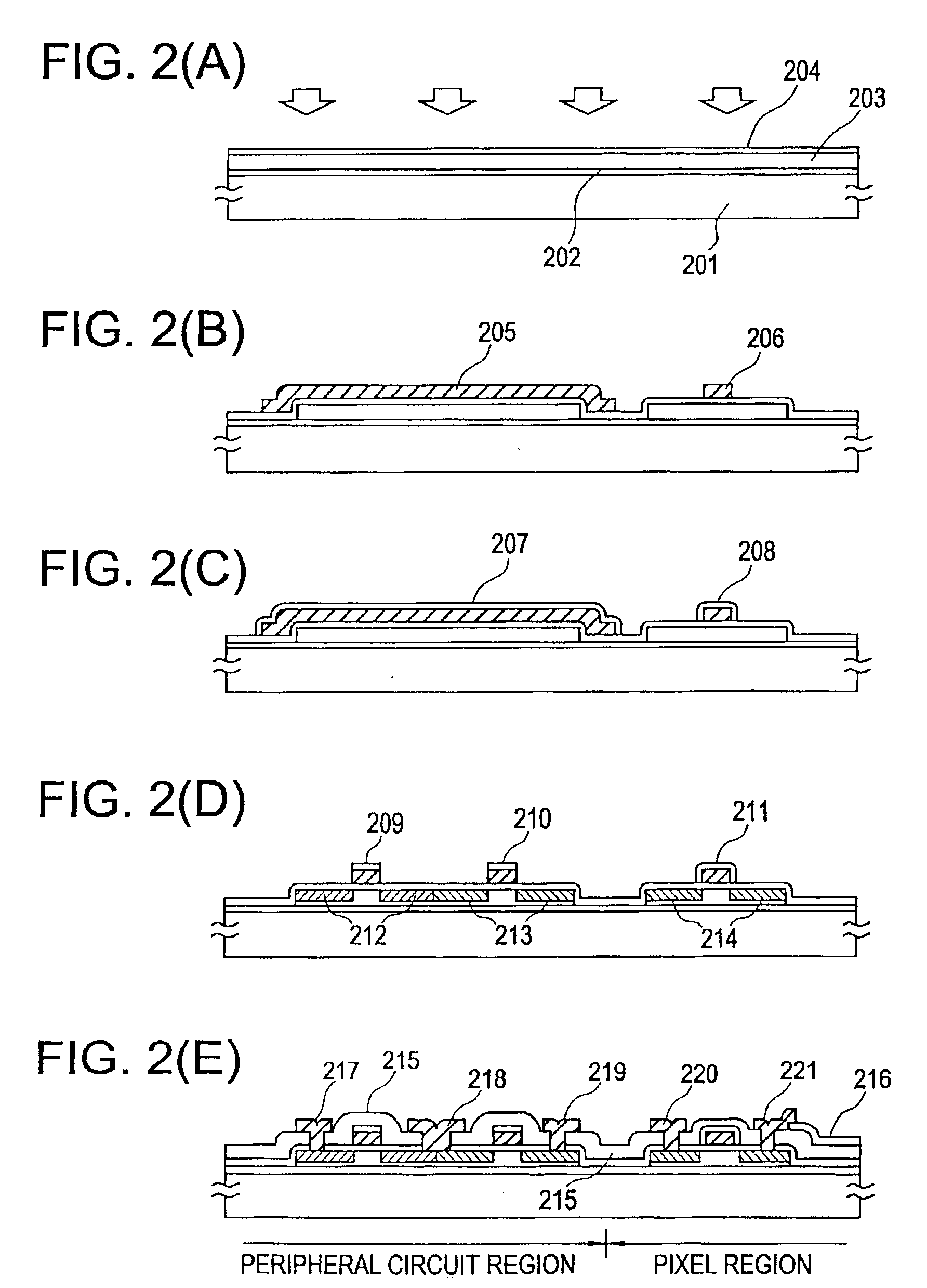
The process sequence of the present example is illustrated in FIG. 2, (A)-(E). A bottom silicon oxide film 202 having a thickness of 100 to 300 nm was formed on an insulating substrate 201 made of Corning 7059 measuring 300 mm×300 mm or 100 mm×100 mm. To form this oxide film, silicon oxide may be sputtered within an oxygen ambient. Alternatively, TEOS is decomposed by plasma CVD and a film is deposited. This film is then annealed at 450 to 650° C.
Thereafter, an amorphous silicon film 203 having a thickness of 30-150 nm, preferably 50-100 nm, was deposited by plasma CVD or LPCVD. A protective layer 204 consisting of silicon oxide or silicon nitride and having a thickness of 20 to 100 nm, preferably 50 to 70 nm, was formed by plasma CVD. Then, as shown in FIG. 2(A), the amorphous silicon film was illuminated with light emitted by a KrF excimer laser producing a wavelength of 248 nm and a pulse width of 20 nsec to improve the crystallinity of the silicon film 203. The energy density of...
example 3
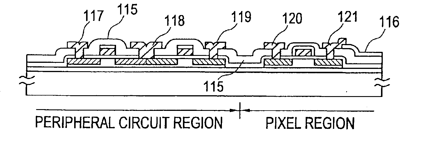
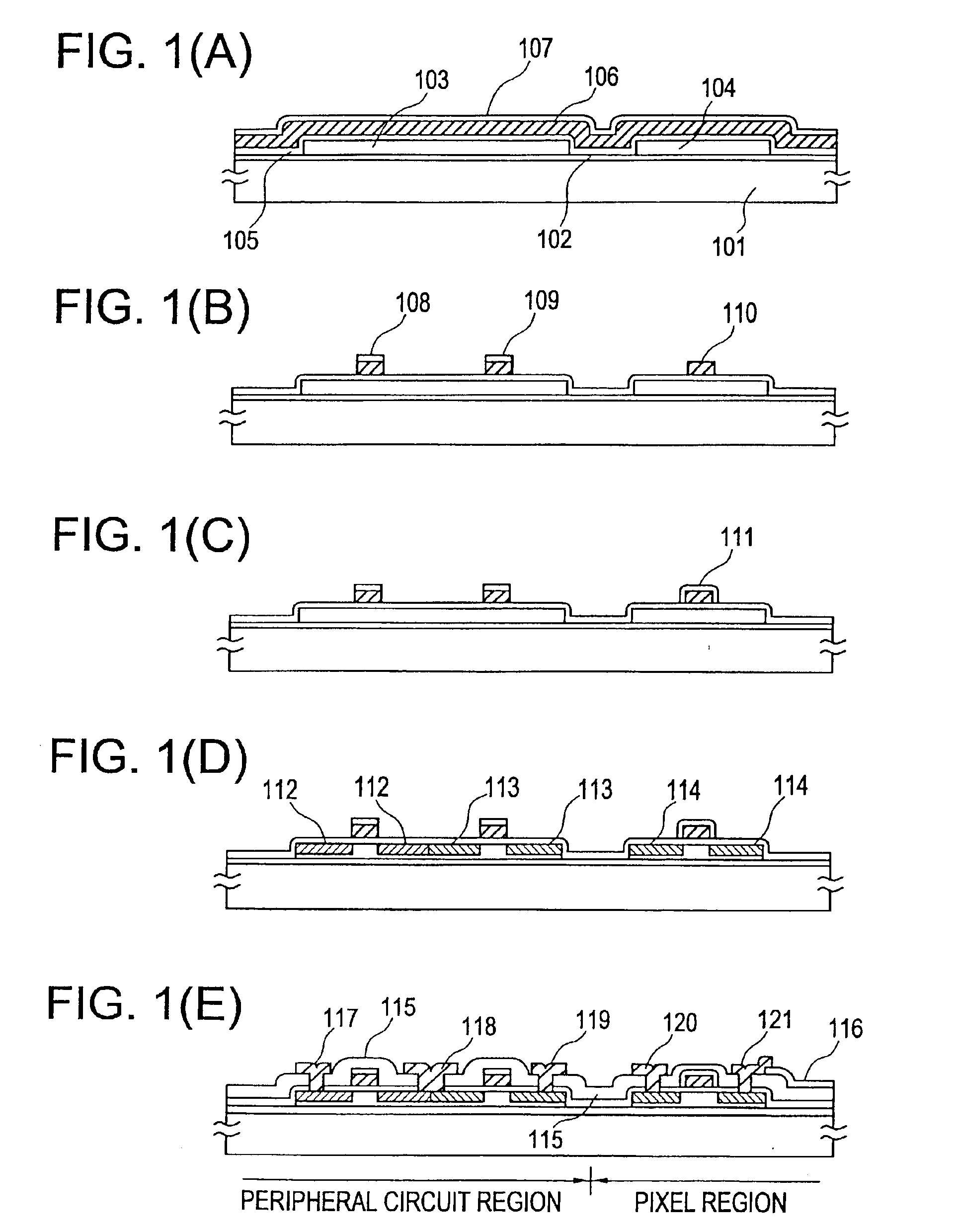
This example is shown in FIG. 1. In the same manner as EXAMPLE 1, a TFT region 103 of a peripheral driving circuit and a TFT region 104 of a matrix circuit are formed of crystalline silicon on a substrate 101 on which a base film 102 has been formed. A gate oxide film 105 of 100 nm thickness is formed by a sputtering method in an oxygen atmosphere. Then an aluminum film 106 of 500 nm thickness is formed on the whole surface of the substrate by electron beam deposition method. This is oxidized by an anodic oxidation method, and anodic oxide 107 of 30 to 300 nm thickness, e.g., 100 nm thickness is formed on the surface. (FIG. 1(A))
As is shown in FIG. 1(B), the anodic oxide is etched with an etchant mainly comprising phosphoric acid (e.g., mixed solution of phosphoric acid, nitric acid, and acetic acid added with a minute amount of chromic acid by approximately 3%). The metal aluminum film 106 is etched by RIE with employing the residual anodic oxide as a mask. Furthermore, a mask is m...
example 4
This example is shown in FIG. 1. In the same manner as EXAMPLE 1, a TFT region 103 of a peripheral driving circuit and a TFT region 104 of a matrix circuit are formed of crystalline silicon on a substrate 101 on which a base film 102 has been formed. A gate oxide film 105 of 100 nm thickness is formed by a sputtering method in an oxygen atmosphere. Then an aluminum film 106 of 500 nm thickness is formed on the whole surface of the substrate by electron beam deposition method. This is oxidized by an anodic oxidation method, and anodic oxide 107 of 30 to 300 nm thickness, e.g. 100 nm thickness is formed on the surface. (FIG. 1(A))
As is shown in FIG. 1(B), the anodic oxide is etched by an etchant mainly comprising phosphoric acid. The metal aluminum film 106 is etched by RIE with employing the residual anodic oxide as a mask. Furthermore, a mask is made in the peripheral circuit portion, and anodic oxide on the gate electrode of the matrix circuit is etched. In this manner, gate electr...
PUM
| Property | Measurement | Unit |
|---|---|---|
| temperature | aaaaa | aaaaa |
| temperature | aaaaa | aaaaa |
| temperatures | aaaaa | aaaaa |
Abstract
Description
Claims
Application Information