Organic semiconductor device having an active dielectric layer comprising silsesquioxanes

a technology of active dielectric layer and organic semiconductor, which is applied in semiconductor devices, solid-state devices, coatings, etc., can solve the problems of conflicting optimization parameters, reducing reliability, and reducing dielectric properties,

Inactive Publication Date: 2005-05-10
ALCATEL-LUCENT USA INC +1
View PDF28 Cites 81 Cited by
  • Summary
  • Abstract
  • Description
  • Claims
  • Application Information

AI Technical Summary

Benefits of technology

[0012]Summarily described, the invention comprises an organic field effect transistor (FET) with an active dielectric layer disposed on a substrate, wherein the active dielectric layer comprises a low temperature cured product of a liquid-deposited silsesquioxane precursor. Referring to FIG. 3, in one embodiment, the invention is directed to an article comprising an organic FET comprising a gate electrode 1 on a substrate 2; an active dielectric layer 3 over the substrate 2; an active semiconducting layer 4 over the active dielectric layer, wherein the active dielectric layer comprises a low-temperature cured high-speed deposition product of at least silsesquioxane precursor; and a source electrode 5 and a drain electrode 6 in contact with the active semiconducting layer. The silsesquioxane precursor is cured to form a high-dielectric strength film of silsesquioxanes. The silsesquioxane precursors preferably comprise alkyl(methyl) and / or alkyl(methyl) phenyl oligomers. The invention also embraces a process for making an organic FET comprising providing a substrate suitable for an organic FET, applying a liquid-phase solution of silsesquioxane precursors over the surface of the substrate; and curing the solution to form a silsesquioxane active dielectric layer. The organic FET thus produced has a high-dielectric, silsesquioxane film with a dielectric constant of greater than about 2, and advantageously, the substrate comprises an indium-tin oxide coated plastic substrate.

Problems solved by technology

As the cell size has shrunk, designers have resorted to extremely thin or non-planar films of a-SiOx, but these films have been problematic as they exhibit a decreased reliability due to finite breakdown fields or have other attendant problems such as step coverage and conformality.
An increase in a material's insulating properties through chemical substitution may, in fact, decrease the dielectric properties.
Thus, the use of silsesquioxanes as low dielectric constant materials for insulating layers of inorganic semiconductor devices presents drawbacks in terms of the processing steps required to achieve suitable materials and conflicting optimization parameters.
However, organic devices provide their own materials constraints, e.g., concerns in developing active materials include their compatibility with and adhesiveness to plastic substrates and stability during processing steps.
Presently-available organic polymers do not meet all the criteria needed for high-performance, low cost organic FETs.
However, most polyimides require high curing temperatures above 200° C., rendering them unsuitable for use with many plastic substrates.
All-polymer logic circuits have been made incorporating poly(vinylphenol), but the current-voltage (I-V) characteristics of these devices tend to change dramatically with time.
Poly(methylmethacrylates) (PMMA) are other organic materials that have been used as dielectrics in organic devices but these tend to have low glass transition temperatures and are easily soluble in other organic solvents used during device processing which is disadvantageous.

Method used


Image

  • Organic semiconductor device having an active dielectric layer comprising silsesquioxanes
  • Organic semiconductor device having an active dielectric layer comprising silsesquioxanes
  • Organic semiconductor device having an active dielectric layer comprising silsesquioxanes

Examples


example 1

Preparation Example

[0035]Plastic substrates suitable for organic FETs were provided and cleaned with acetone, methanol, and de-ionized water. The substrate surfaces were treated with RIE using oxygen plasma for one minute at 50 W. The substrates were taped to glass slides using KAPTON® tape before spin coating, and then again cleaned by applying isoproponal while spinning the substrate at 3000 rpm. A glass resin solution (e.g., comprising GR150 dissolved in n-butanol at a concentration of 25 wt % n-butanol with 1 wt % A110) was filtered once through a syringe filter with a pore size of 0.45 μm, and then twice through filters having a pore size of 0.19 μm, and dispensed on the substrates following by spinning at 1000 to 3000 rpm for one minute. The entire substrate was covered with the filtered solution and then spun at 1000 to 3000 rpm for one minute. (Preferred results are achieved when the solution is deposited so as to cover the entire substrate surface.)

[0036]The resultant subst...

example 2

Capacitance Values

[0037]Capacitance values for films produced according to the invention and the steps set forth in Example 1 are recorded below in Table 1.

[0038]

TABLE 1Capac-SpinitanceSilsesquioxaneConcentration ofRate(nF / materialsilsesquioxanes(rpm)Substratecm2)GR 15025 wt % in n-butanol3KSiO2 (1000 Å)2.14(methylphenyl)25 wt % in n-butanol3KITO / Mylar ®4.9725 wt % A11001KITO / Mylar ®2.74(1 wt %)GR T63060 wt % in methanol3KITO / glass0.43(methylphenyl anddimethyl)GR 710Unknown, use as3KITO / Mylar ®19.11(methylrec'd, in n-butanolphenyl)Unknown, use as1KITO / Mylar ®11.72rec'd, in n-butanolGR 72013 wt % in propyl3KITO / Mylar ®7.03(methylpropasolphenyl)13 wt % in propyl1KITO / Mylar ®4.08propasolGR 653 LPP31 wt % in n-butanol3KITO / glass0.8731 wt % in n-butanol4KITO / Mylar ®2.4231 wt %, A11003KITO / Mylar ®1.59(1 wt %) in n-butanolGR 653L30 wt %3KITO / glass0.75

[0039]As can be seen, the capacitance values differed depending upon the type of silsesquioxane precursors, the film thickness, the degree of...

example 3

FET Performance as a Function of Semiconducting Material

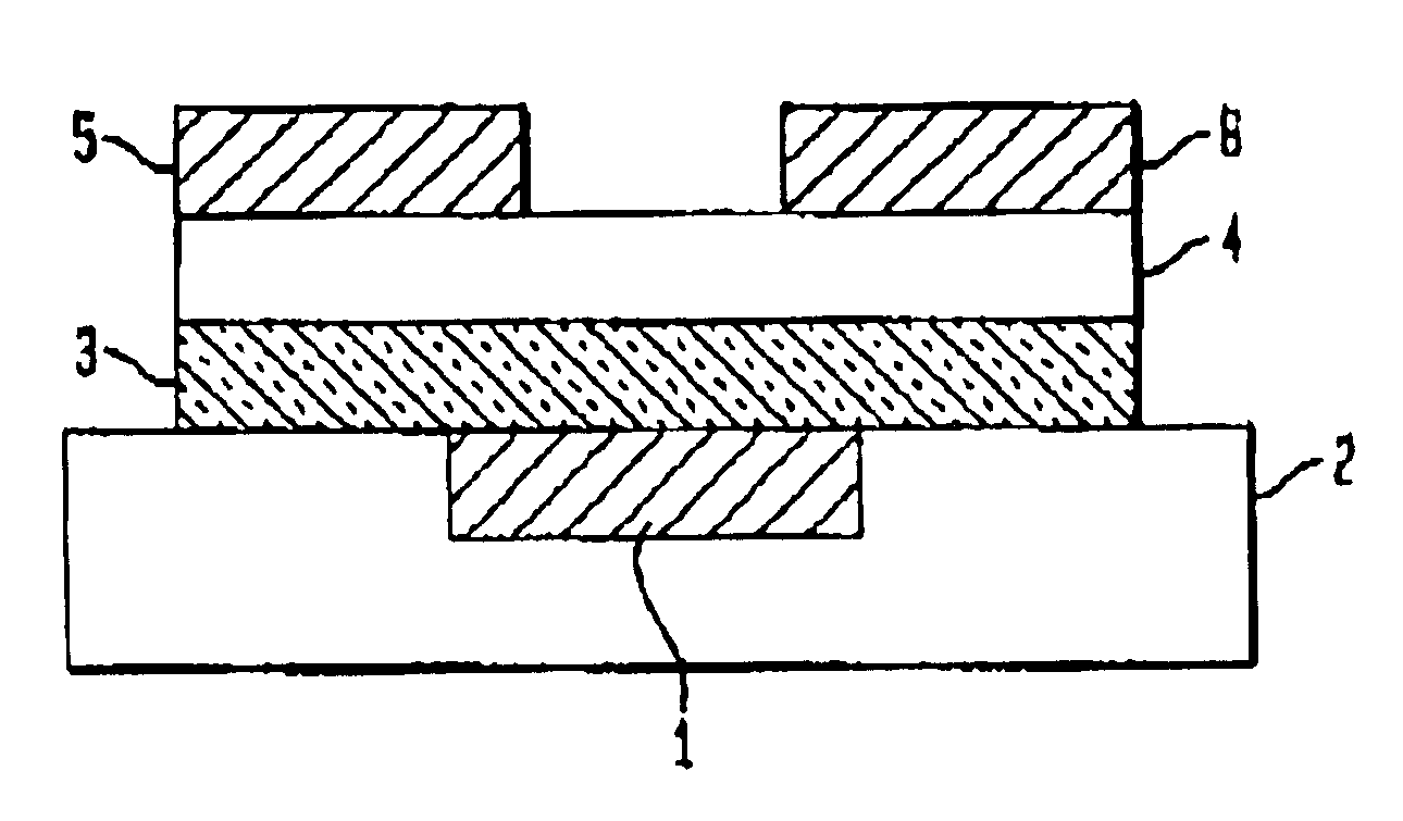
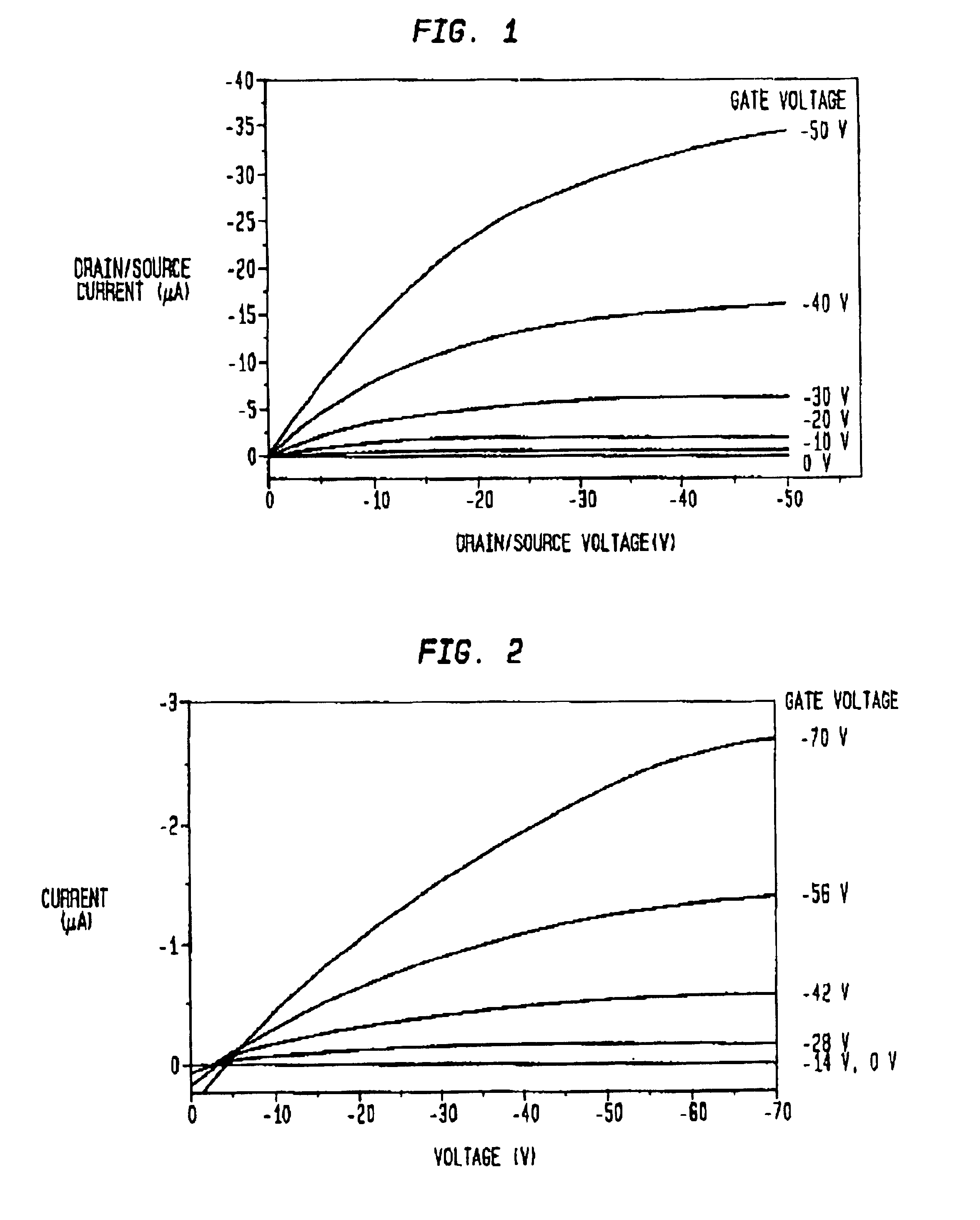
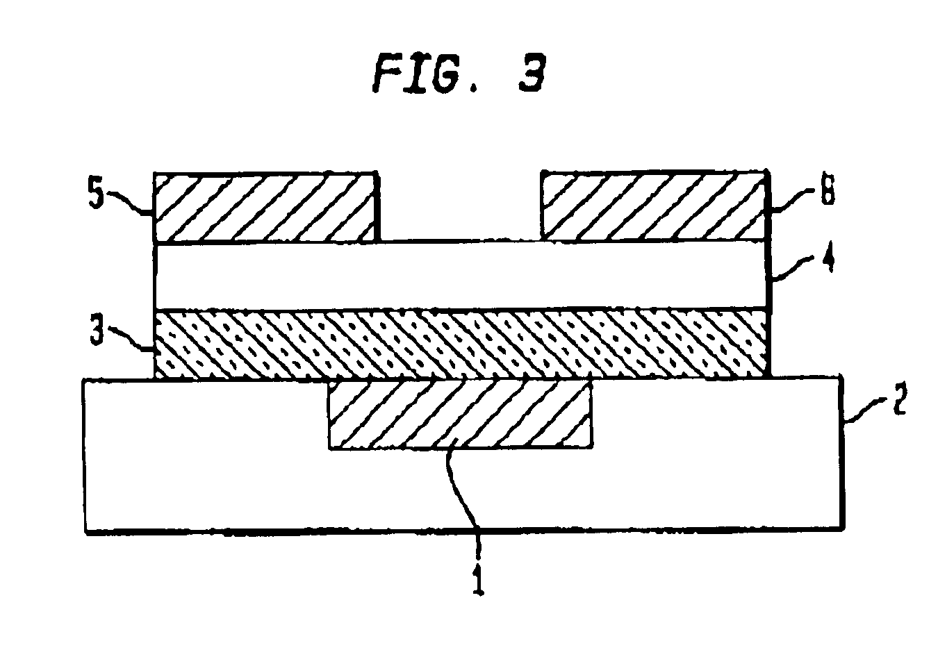
[0040]The inventors evaluated the field-effect transistor performance of the inventive devices using six different organic semiconducting materials. The performance of these devices compared to the performance of devices having a polyimide or SiO2 as the active dielectric layer. Top-contact geometry devices were prepared having dielectric films prepared from liquid-deposited silsesquioxane precursors as described in Example 1, that had been deposited on one of six organic semiconducting materials. In most cases, the substrate used was an ITO-coated MYLAR® plastic substrate, although in some instances a SiO2 / Si substrate was used, as noted below in Table 2. The material for fabricating the active semiconducting layer in each of these devices was selected from one of the following materials: n-channel vacuum evaporated hexadecafluoro copper phthalocyanine (FCuPc); p-channel vacuum evaporated copper phthalocyanine (CuPc), α-sexith...


PUM

PropertyMeasurementUnit
dielectric constantaaaaaaaaaa
pore sizeaaaaaaaaaa
thicknessaaaaaaaaaa

Abstract

An organic field effect transistor (FET) is described with an active dielectric layer comprising a low-temperature cured dielectric film of a liquid-deposited silsesquioxane precursor. The dielectric film comprises a silsesquioxane having a dielectric constant of greater than 2. The silsesquioxane dielectric film is advantageously prepared by curing oligomers having alkyl(methyl) and/or alkyl(methyl) pendant groups. The invention also embraces a process for making an organic FET comprising providing a substrate suitable for an organic FET; applying a liquid-phase solution of silsesquioxane precursors over the surface of the substrate; and curing the solution to form a silsesquioxane active dielectric layer. The organic FET thus produced has a high-dielectric, silsesquioxane film with a dielectric constant of greater than about 2, and advantageously, the substrate comprises an indium-tin oxide coated plastic substrate.

Description

FIELD OF THE INVENTION[0001]The present invention relates to an organic semiconductor device having an active dielectric layer fabricated with a liquid-deposited, high dielectric strength silsesquioxane.BACKGROUND OF THE INVENTION[0002]The metal-oxide semiconductor field-effect transistor (MOSFET or MOS device) is a dominant and important device in fabricating memory devices and integrated circuits, and various types of MOSFETS are known. MOSFET technology includes NMOS, PMOS, and CMOS technology. NMOS and PMOS devices are n-channel and p-channel devices, respectively, and CMOS devices comprise n-channel and p-channel devices integrated on the same chip. Other acronyms used to identify MOSFETs include DMOS (wherein “D” stands for “diffusion” or “double diffusion”), IGBT (Insulated Gate Bipolar Transistor), BiCMOS (CMOS having bipolar devices), and DGDMOS (Dual Gate DMOS).[0003]There is a continuing desire in the microelectronics industry to miniaturize device components, increase th...

Claims


Application Information

Patent Timeline
Patent Type & Authority Patents(United States)
IPC IPC(8): H01L21/02H01L21/312H01L51/05H01L51/30H01L29/76H01L51/00
CPCH01L51/0516H01L21/3124H01L51/0036H01L51/0545H01L51/0078H01L51/0052H01L21/02137H01L21/02282H01L21/02315H01L21/02216H10K85/113H10K85/615H10K85/311H10K10/468H10K10/466
Inventor BAO, ZHENANKUCK, VALERIE JEANNEPACZKOWSKI, MARK ANTHONY
Owner ALCATEL-LUCENT USA INC
Why Eureka
Try Eureka