Polycrystalline germanium-based waveguide detector integrated on a thin silicon-on-insulator (SOI) platform

a technology of thin silicon and waveguide detector, applied in the field of optical detectors, can solve the problems of lack of available component integration, high cost, high power consumption, etc., and achieve the effects of low dark current operation, high speed, and efficient collection

Active Publication Date: 2005-05-24
CISCO TECH INC
View PDF5 Cites 83 Cited by
  • Summary
  • Abstract
  • Description
  • Claims
  • Application Information

AI Technical Summary

Benefits of technology

[0008]In particular, the present invention relates to various poly-germanium-based photodetector structures that are monolithically integrated with relatively thin silicon waveguides formed in an SOI platform. Poly-germanium may be formed using various techniques such as, but not limited to, physical vapor deposition (PVD) or chemical vapor deposition (CVD). In SOI-based thin silicon waveguides, the optical mode is tightly confined, due to the large index contrast (nSi=3.5 and nSiO2=1.5). In accordance with the present invention, the light propagating in a silicon waveguide, upon reaching the region with the overlying poly-germanium layer undergoes absorption into the poly-germanium. The band gap of germanium (˜0.72 eV) ensures effective absorption of near-IR wavelength light. The electron-hole pairs generated due to the absorption of light can be efficiently collected using suitable electrode structures fabricated upon the poly-germanium layer. The physical dimensions of the poly-germanium layer (i.e., height, width and length) are used to control the amount of light that is absorbed.
[0009]In a preferred embodiment of the poly-germanium detector of the present invention, the detector layer is formed as a wrap-around geometry over a silicon strip waveguide formed on an SOI platform, with contacts formed on either side of the strip for biasing the detector. The narrow lateral waveguide dimensions (˜1 μm) allow for high speed, low dark current operation with a high responsivity, due to a significantly smaller area when compared to normal incidence detectors.

Problems solved by technology

One of the reasons for the high cost, high power consumption and large form factors of the optical components / subsystems in the optical communication industry is the lack of available component integration.
Similar to the IC industry in the 1960s, these discrete components are open loop, where the loop is then closed externally (using, for example, external optics and electronics), resulting in lower yields and higher costs.
The majority of the InGaAs-based detectors are normal incidence detectors, and integration of such devices on silicon surfaces is expensive.
Germanium detectors exhibit a higher dark current than InGaAs-based detectors, which limit their application in the telecommunications industry.

Method used


Image

  • Polycrystalline germanium-based waveguide detector integrated on a thin silicon-on-insulator (SOI) platform
  • Polycrystalline germanium-based waveguide detector integrated on a thin silicon-on-insulator (SOI) platform
  • Polycrystalline germanium-based waveguide detector integrated on a thin silicon-on-insulator (SOI) platform

Examples


Embodiment Construction

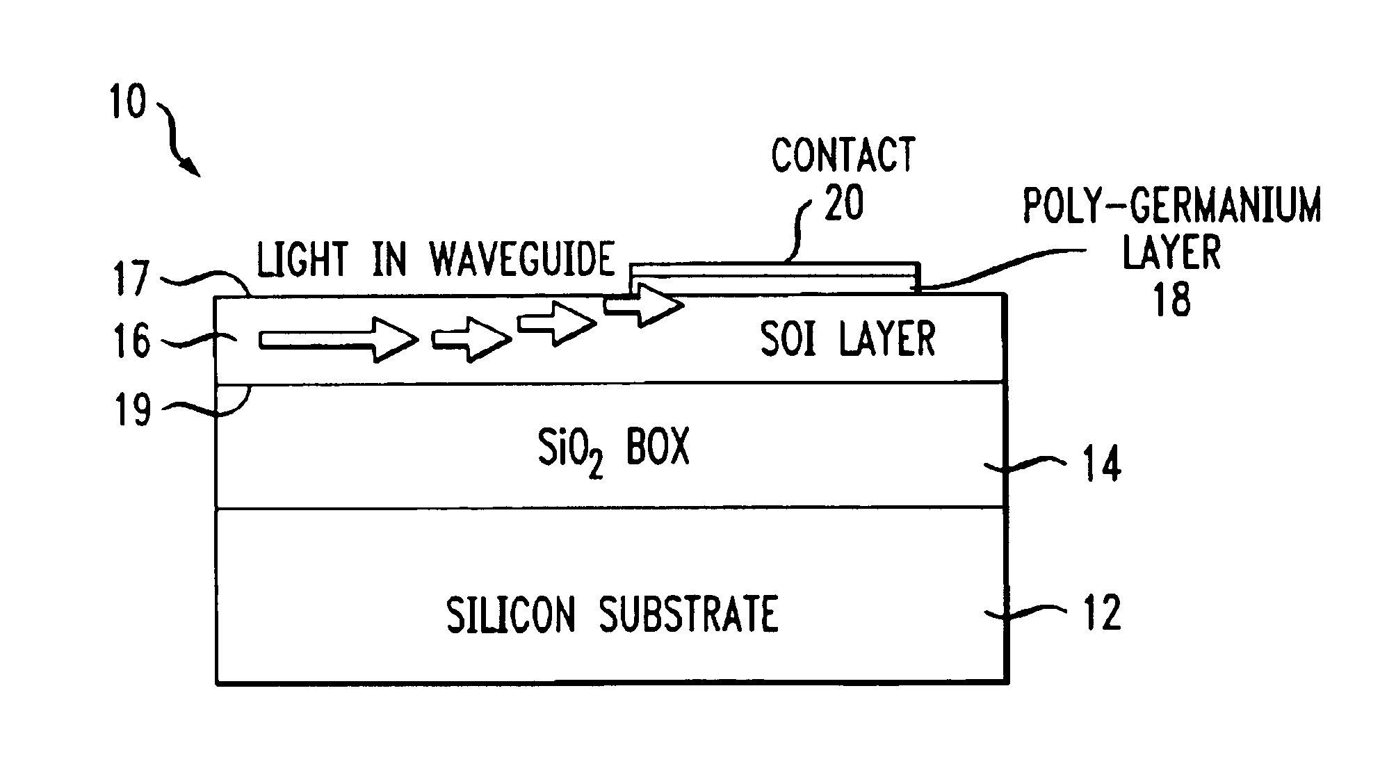
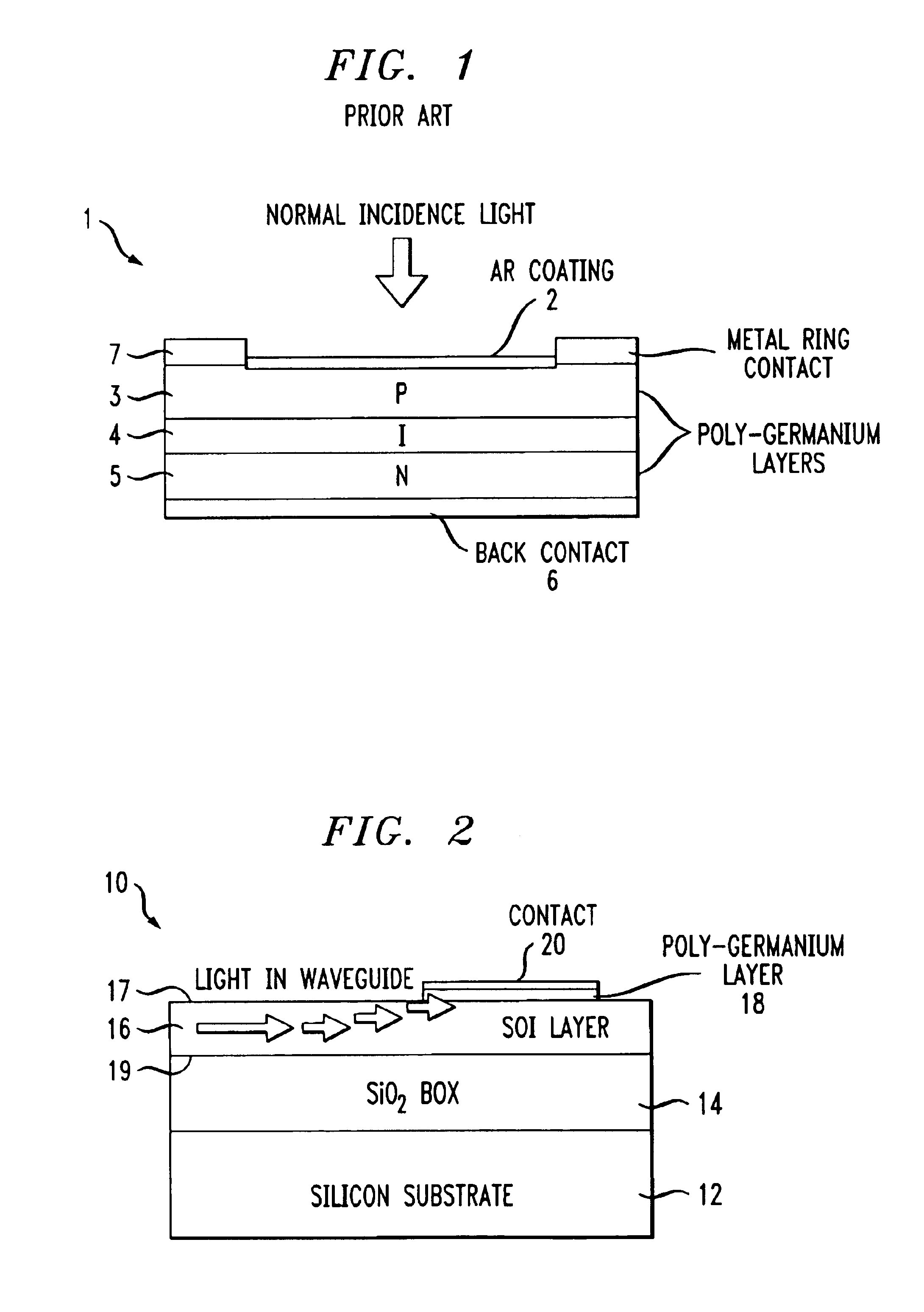
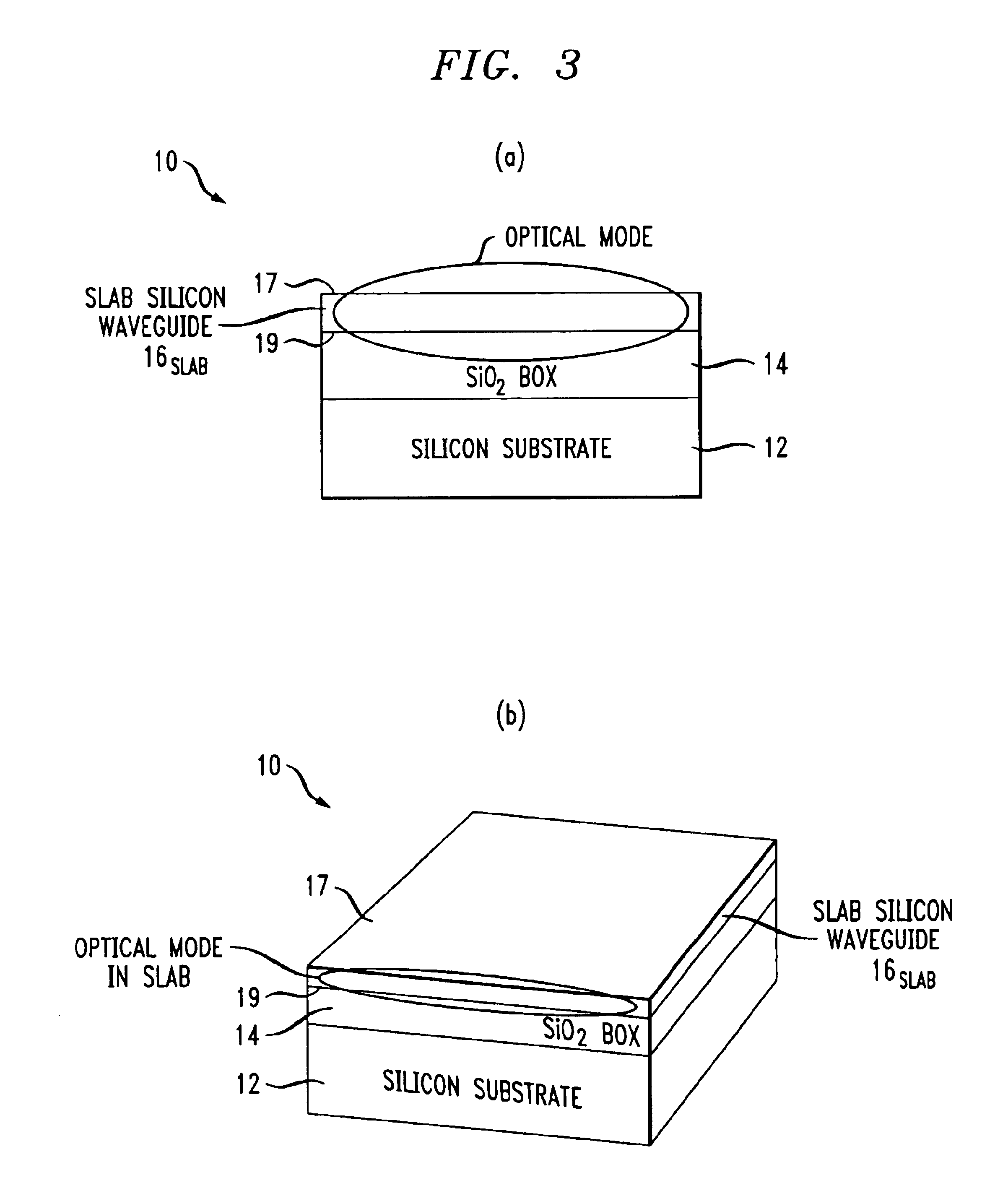
[0030]Prior to describing in detail the poly-germanium SOI-based photodetector of the present invention, it is useful to briefly describe the working of a conventional, normal incidence photodetector. FIG. 1 illustrates, in cross-sectional view, one such conventional prior art detector 1. Detector 1 is considered a “normal” incidence photodetector since the direction of the incoming light beam is perpendicular to the plane of the impinging surface, in this case, an AR coating layer 2. Detector 1 is a p-i-n photodetector comprising a p-doped poly-germanium layer 3, an intrinsically doped layer 4 and an n-doped layer 5. The electrical contacts are formed on opposing sides of detector 1, as shown, with a bottom contact 6 and a top, ring-shaped contact 7. The thickness and doping of layers 3, 4 and 5 determine the amount of light absorbed and the speed of response of detector 1. The absorption area within p-doped layer 3 is typically on the order of 100 μm2 (the larger absorption area r...


PUM


Abstract

A photodetector for use with relatively thin (i.e., sub-micron) silicon optical waveguides formed in a silicon-on-insulator (SOI) structure comprises a layer of poly-germanium disposed to couple at least a portion of the optical signal propagating along the silicon optical waveguide. Tight confinement of the optical signal within the waveguide structure allows for efficient evanescent coupling into the poly-germanium detector. The silicon optical waveguide may comprise any desired geometry, with the poly-germanium detector formed to either cover a portion of the waveguide, or be butt-coupled to an end portion of the waveguide. When covering a portion of the waveguide, poly-germanium detector may comprise a “wrap-around” geometry to cover the side and top surfaces of the optical waveguide, with electrical contacts formed at opposing ends of the detector.

Description

CROSS-REFERENCE TO RELATED APPLICATION[0001]This application claims the benefit of Provisional Application No. 60 / 459,348, filed Mar. 31, 2003.TECHNICAL FIELD[0002]The present invention related to optical detectors and, more particularly, to a polycrystalline germanium-based waveguide detector integrated on a thin silicon-on-insulator (SOI) platform.BACKGROUND OF THE INVENTION[0003]In an SOI-based opto-electronic platform, relatively thin (e.g., <1 μm) silicon waveguides are used to distribute light across the entire chip and provide multiple optical functions (for example, splitting / combining, modulation, switching, wavelength multiplexing / demultiplexing, add / drop, equalization, and dispersion compensation). The ability for light coupling and manipulation in a thin waveguide on an SOI platform enables a true integration of optics and microelectronics on a single silicon chip. One of the reasons for the high cost, high power consumption and large form factors of the optical compo...

Claims


Application Information

Patent Timeline
Patent Type & Authority Patents(United States)
IPC IPC(8): H01L21/02H01L27/148H01L21/302H01L31/00H01L
CPCB82Y20/00G02B6/1225G02B6/1226H01L31/0232G02B6/125G02B6/1228G02F1/025G02F2201/58H01L31/02327H01L31/035281H01L31/03682H01L31/1808H01L27/12H01L27/13Y02E10/546
Inventor GOTHOSKAR, PRAKASHGHIRON, MARGARETPATEL, VIPULKUMARMONTGOMERY, ROBERT KEITHSHASTRI, KALPENDUPATHAK, SOHAMYANUSHEFSKI, KATHERINE A.
Owner CISCO TECH INC
Why Eureka
Try Eureka