Laser processing method to a class substrate and an optical diffraction element obtained thereby, and a method for manufacturing optical elements

a technology of optical diffraction elements and laser processing methods, which is applied in the direction of manufacturing tools, transportation and packaging, coatings, etc., can solve the problems of large-scale facilities, inconvenient operation, and disadvantageous limit of humidity resistance and excessive temperature, and achieve the effect of reducing reflectivity

Inactive Publication Date: 2005-08-02
NIPPON SHEET GLASS CO LTD
View PDF23 Cites 32 Cited by
  • Summary
  • Abstract
  • Description
  • Claims
  • Application Information

AI Technical Summary

Benefits of technology

[0038]As a source of the laser beam, an excimer laser such as KrF, an Nd-YAG laser, a Ti:Al2O3 laser and the high harmonics thereof, or a pigment las...

Problems solved by technology

However, there is a problem with the care and the treatment of the etchant in the wet etching, and also a problem in the dry etching in that the facility of a vacuum container is necessitated, thereby requiring a large-scale facility by itself.
Additionally, it is not cost-effective because a pattern mask and the like must be formed by a further complicated photolithography technique.
The transfer onto the ...

Method used


Image

  • Laser processing method to a class substrate and an optical diffraction element obtained thereby, and a method for manufacturing optical elements
  • Laser processing method to a class substrate and an optical diffraction element obtained thereby, and a method for manufacturing optical elements
  • Laser processing method to a class substrate and an optical diffraction element obtained thereby, and a method for manufacturing optical elements

Examples


embodiment 1

[0050

[0051]On a soda-lime glass there is formed an SiO2 thin layer or film, in which colloidal Ag is dispersed. As a method for forming, there is used a sputtering method, in which an SiO2 target and a chip of silver metal are positioned on a target and are sputtered at the same time. The sputtering condition is set as below for growing a film. And, as the target, there is used a quartz target which is positioned below and which has a size of 5 inches×20 inches, on which thirty two (32) disc-shaped chips of silver (having diameters of about 4 mm) are positioned in dispersed locations.

[0052]Sputtering Condition:

[0053]Gas flow: Oxygen 3 sccm, Argon 97 sccm

[0054]Pressure when sputtering: 2.8×10⁻³ Torr

[0055]Applied electric power: 3.0 kW

[0056]Substrate: Soda lime glass

[0057]The thin film obtained is a clear film which is brown colored, and has a flat surface and strong adhesion. The film grows to be 315 nm in thickness with 5 minutes of film growing time. And, a concentration of silver ...

embodiment 6

[0076

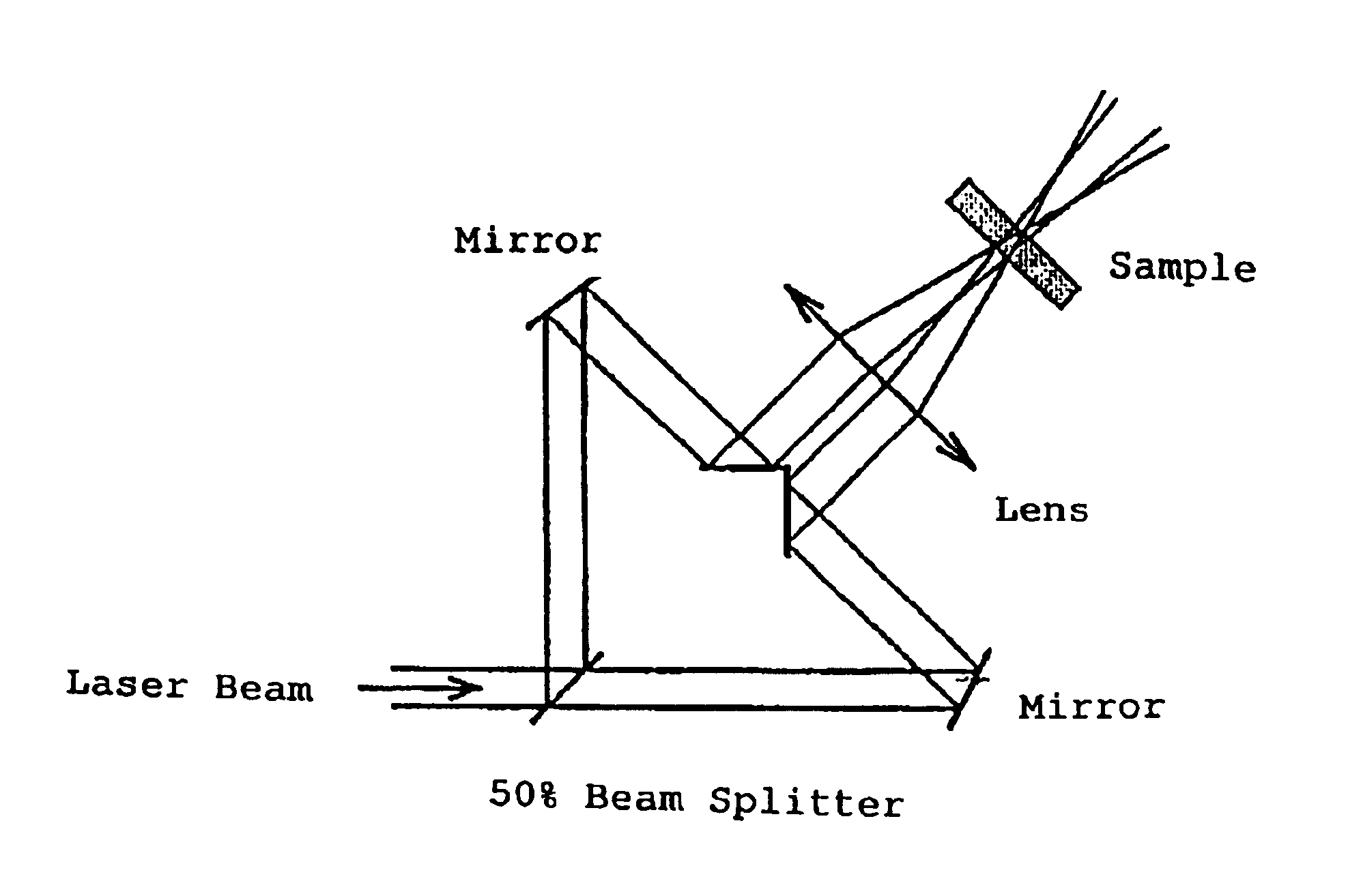
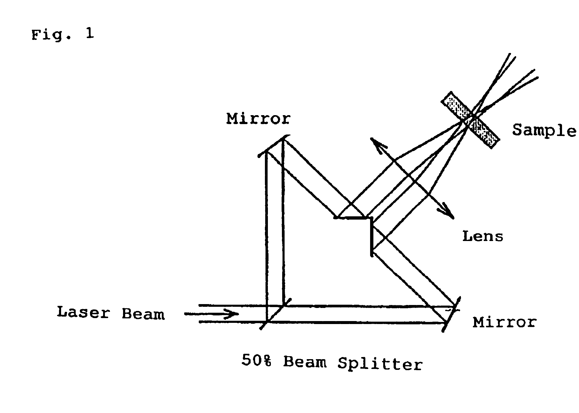
[0077]A diffraction grating is manufactured on the same sample used in Embodiment 2, by using the apparatus shown in FIG. 4. In more detail, on the film surface of the Ag—SiO2 film formed on the above glass substrate, there is positioned a substrate having a phase mask, on which the diffraction grating is formed, through a spacer, and then the laser beam is irradiated onto it.

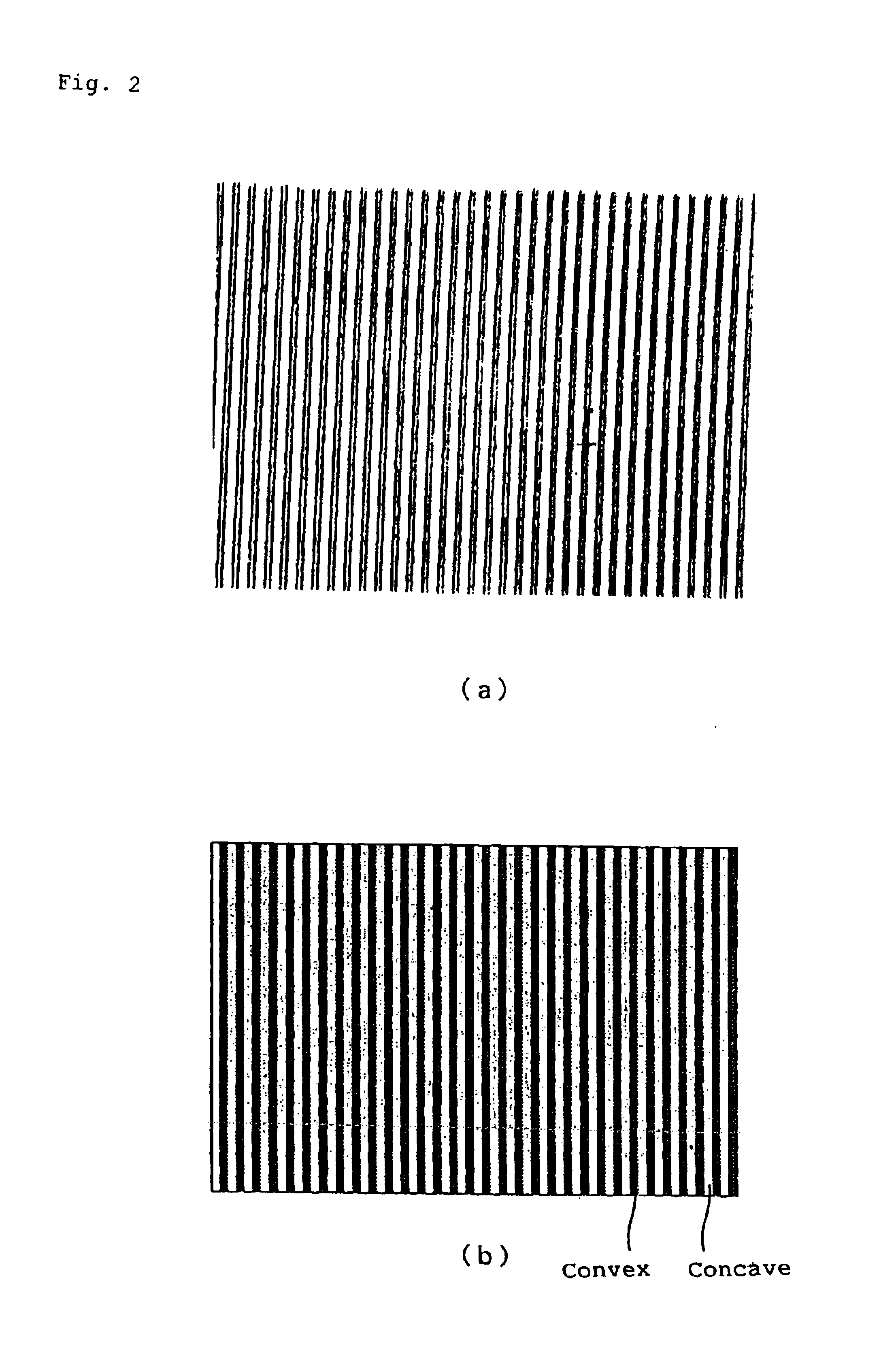
[0078]With the irradiation of the laser beam upon the phase mask, as shown in FIG. 5(a), a plurality of diffraction light beams mainly included in an arc corresponding to +1 degree, 0 degree and −1 degree are emitted therefrom, then, by the mutual interference of the diffracted light beams, a periodic distribution of optical intensity is obtained in the vicinity of the emission side of the phase mask.

[0079]In the present embodiment, there is used a phase mask having a diffraction grating frequency of 1055 nm, a depth of the diffraction grating being about 250 nm, and a size of 10 mm×5 mm (made by QPS Techn...

embodiment 9

[0086

[0087]On a soda-lime glass substrate there is formed a TiO2 thin film, into which colloidal gold is dispersed by a sol-gel method. As materials of manufacturing, the thin film mainly includes titan tetrabutoxyde (TTB), with which is mixed acetylacetone (AA) of 4-times equivalent mol weight. This is helpful to obtain a thin film of good quality, since it proceeds hydrolysis of water which participates in the main reaction of the sol-gel reaction. As a reacting solution for the hydrolysis, there is used an aqueous solution of NaAuCl4 dissolved at a concentration of 0.16 mol / l. After the reaction by combining and agitating 12 ml of TTB, 12 ml of ethanol for dilution, 4 ml of AA and an aqueous solution of 3 ml of NaAuCl4 for thirty (30) minutes, the resulting solution is painted on the glass substrate by a dip method. After the painting, it is heated for fifteen (15) minutes in air at 400° C. so as to evaporate the remaining organic materials and to obtain a sticky film. In this ca...


PUM

PropertyMeasurementUnit
Angleaaaaaaaaaa
Angleaaaaaaaaaa
Lengthaaaaaaaaaa

Abstract

In a laser processing method for accurately forming a convexo-concave structure on the surface of a glass substrate, a periodic optical intensity distribution of a laser beam is obtained by an interference between diffracted light beams of +1 degree and −1 degree emitted from a phase mask, onto which the laser beam is irradiated, in the vicinity of the emission side of the phase mask, and a glass substrate, on which a thin film is formed, is set in the area where the periodic optical intensity distribution is provided. As a result, the thin film is evaporated or ablated depending on the periodic optical intensity, thereby a diffraction grating, which has the same period as that of the varying optical intensity, is formed on the glass substrate.

Description

[0001]This application is a divisional of application Ser. No. 09 / 898,239, filed Jul. 3, 2001, now U.S. Pat. No. 6,645,603 which is a divisional of Ser. No. 09 / 284,269, filed Jun. 4, 1999, now issued U.S. Pat. No. 6,291,797, which is a National Stage Application of PCT / JP97 / 02806 filed Aug. 11, 1997, which application(s) are incorporated herein by reference.BACKGROUND OF THE INVENTION[0002]1. Field of the Invention[0003]The present invention relates to a laser processing method for processing a micro convexo-concave structure on a surface of a glass substrate and an optical diffraction element obtained by the laser processing method, and to a method for manufacturing an optical element including a diffraction grating which is used as a polarized light beam splitter, a coupling grating or the like, a diffraction type optical element which is used for a hologram, or an optical element such as a photonic crystal which is used as a birefringent plate, a light beam scatter plate or the l...

Claims


Application Information

Patent Timeline
IPC IPC(8): B23K26/06C03C17/23C03C23/00C03C17/34
CPCB23K26/0656C03C17/23C03C17/3417C03C17/3452C03C23/0025Y10T428/24273C03C2217/213C03C2218/32C03C2218/328Y10T428/2457C03C2217/212B23K26/066
Inventor KOYAMA, TADASHITSUNETOMO, KEIJI
Owner NIPPON SHEET GLASS CO LTD
Why Eureka
Try Eureka