Manufacturing methods for semiconductor devices with multiple III-V material layers

a technology of iii-v material and fabrication method, which is applied in the direction of crystal growth process, polycrystalline material growth, chemically reactive gas growth process, etc., can solve the problems of high electric field breakdown, direct band gap structure, high thermal conductivity, etc., and achieve the effect of preventing thermal shock, reducing or completely disrupting the epitaxial growth rate, and controlling the conductivity of each layer

Inactive Publication Date: 2005-10-18
OSTENDO TECH INC
View PDF40 Cites 52 Cited by
  • Summary
  • Abstract
  • Description
  • Claims
  • Application Information

AI Technical Summary

Benefits of technology

[0011]According to one aspect of the invention, a method for fabricating multi-layer Group III nitride semiconductor devices in a single reactor run utilizing HVPE techniques is provided, wherein the layers can be either thin (e.g., submicron) or thick (e.g., greater than 1 micron and preferably less than 100 microns). Preferably an atmospheric, hot-walled horizontal furnace is used. Sources (Group III metals, Group V materials, acceptor impurities, donor impurities) are located within the multiple source zones of the furnace, the sources used being dependent upon the desired compositions of the individual layers. Preferably HCl is used to form the necessary halide metal compounds and an inert gas such as argon is used to transport the halide metal compounds to the growth zone where they react with ammonia gas. As a result of the reaction, epitaxial growth of the desired composition occurs. By controlling the inclusion of one or more acceptor and / or donor impurities, the conductivity of each layer can be controlled.
[0012]In at least one embodiment of the invention, the reactor includes one or more gas inlet tubes adjacent to the growth zone. By directing the flow of a gas (e.g., an inert gas) generally in the direction of the substrate's surface and / or in a direction opposite to or in an oblique angle to that the of the gas flow from the source tubes, the epitaxial growth rate can be reduced or completely disrupted.
[0013]In at least one embodiment of the invention, the reactor includes multiple growth zones. Preferably the reactor also includes at least one growth interruption zone. One or more gas inlet tubes direct a flow of gas (e.g., an inert gas) towards the growth interruption zone, thereby substantially preventing any reactive gases from entering into this zone. In use, after the growth of a layer is completed, the substrate is transferred from the growth zone to either the growth interruption zone or to another growth zone. Preferably the temperature of the substrate is maintained during the transfer as well as when the substrate is within the growth interruption zone, thus preventing thermal shock. If the reactor includes a single growth zone, the substrate is transferred to the growth interruption zone so that the growth zone can be purged and the sources required for the next desired layer can be delivered to the growth zone. Preferably the substrate is never transferred to a new growth zone, or from the growth interruption zone to the single growth zone, until the reaction in the intended growth zone has stabilized.

Problems solved by technology

In particular, these materials exhibit a direct band gap structure, high electric field breakdown, and high thermal conductivity.
Although the MOCVD technique has proven adequate for a variety of commercial devices, the process has a number of limitations that constrain its usefulness.
First, due to the complexity of the various sources (e.g., trimethylaluminum, trimethylgallium, and biscyclopentiadienylmagnesium), the process can be very expensive and one which requires relatively complex equipment.
Second, the MOCVD technique does not provide for a growth rate of greater than a few microns per hour, thus requiring long growth runs.
The slow growth rate is especially problematic for device structures that require thick layers such as high voltage rectifier diodes that often have a base region thickness of approximately 30 microns.
Conventional HVPE techniques have been unable, however, to grow such layers.
As a result, the potential of the HVPE technique for fabricating devices based on Group III semiconductors has been limited.

Method used


Image

  • Manufacturing methods for semiconductor devices with multiple III-V material layers
  • Manufacturing methods for semiconductor devices with multiple III-V material layers
  • Manufacturing methods for semiconductor devices with multiple III-V material layers

Examples


embodiment i

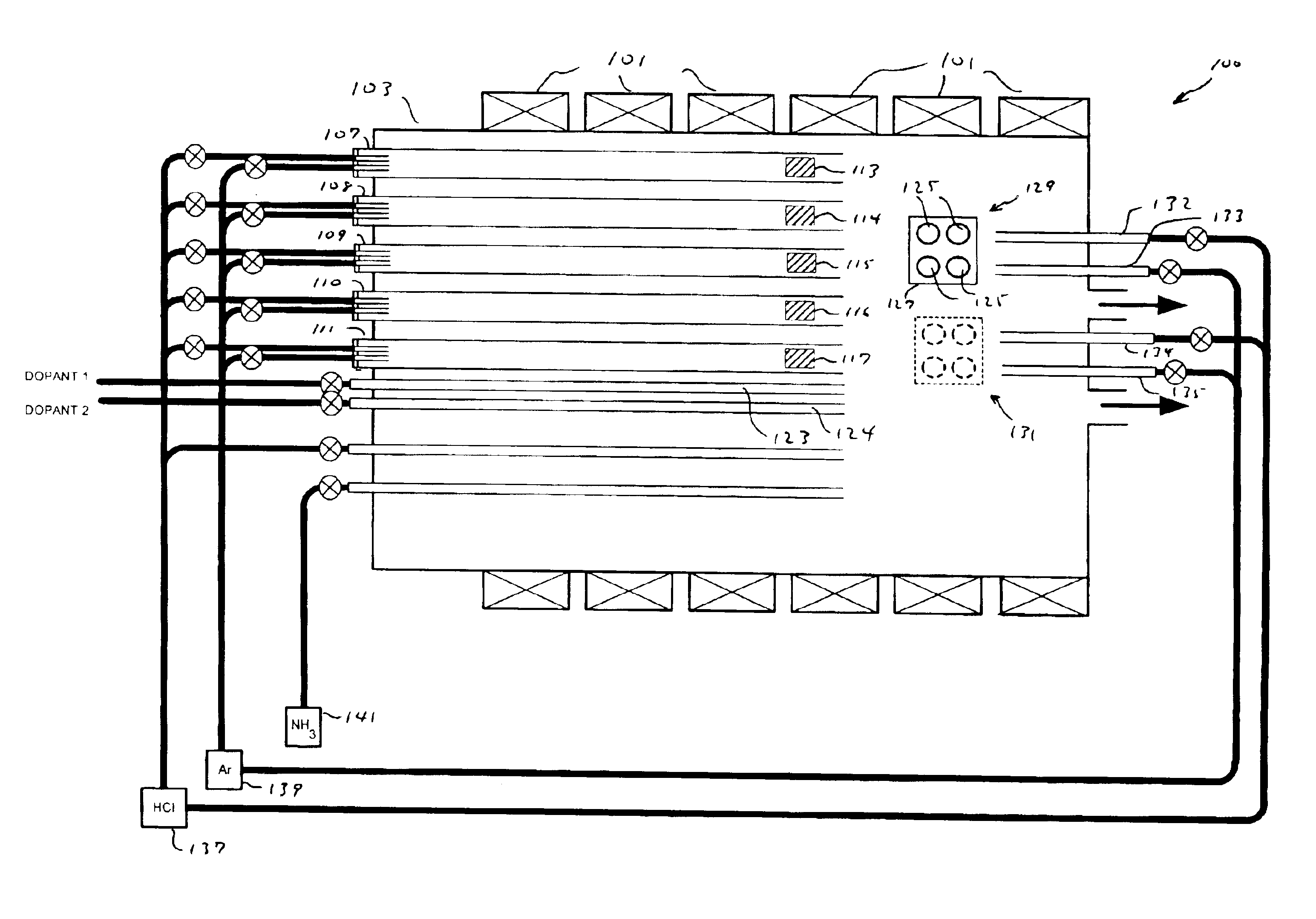
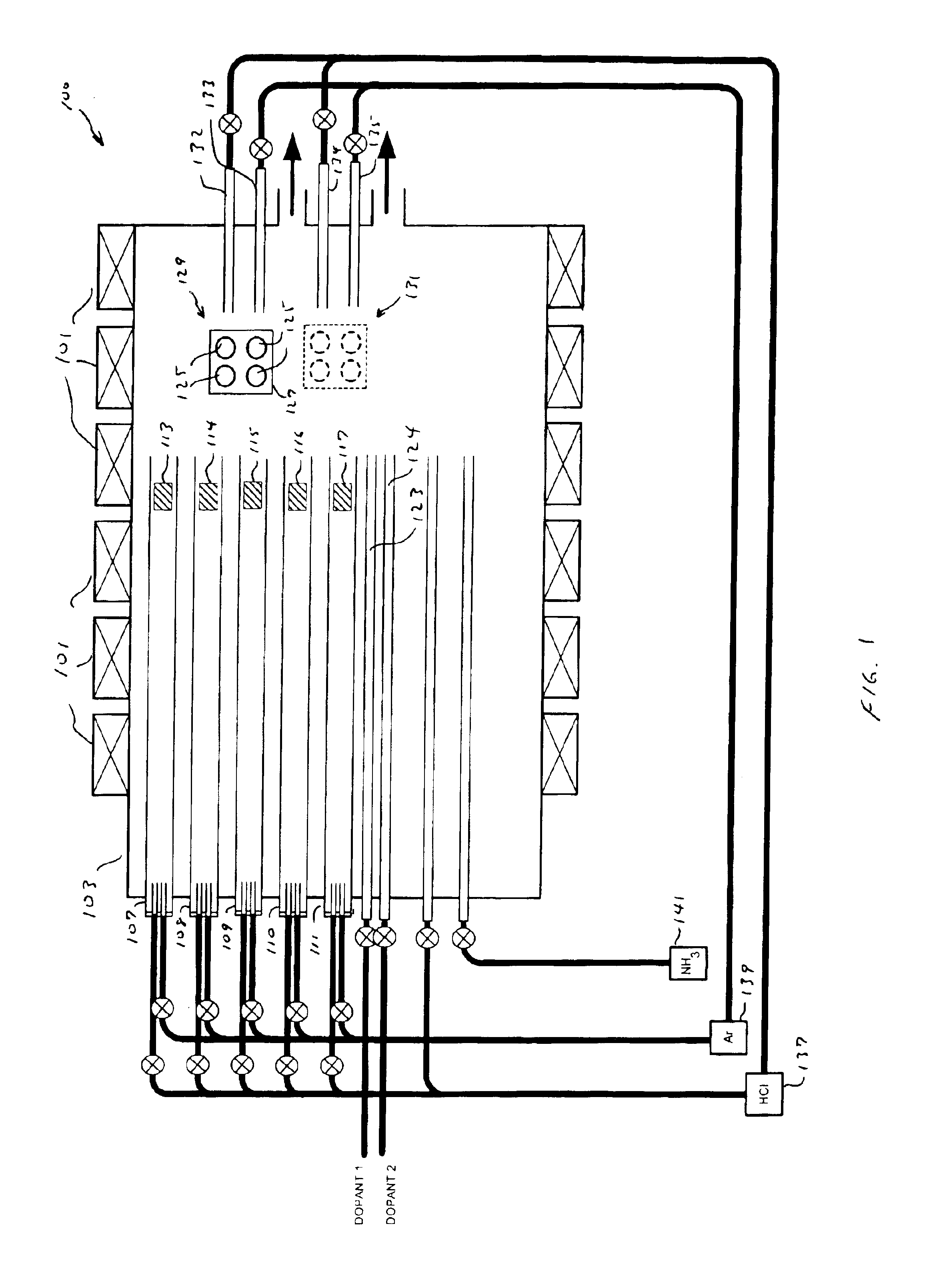
[0049]A 4 inch sapphire substrate with a (0001) surface orientation was loaded into an HVPE reactor. The reactor and sources were prepared as noted above in preparation for the growth of a p-type GaN layer. A growth rate of 1 micron per minute was observed. After a total of fifteen minutes, the sample was removed from the growth zone. No cracks were visible in the resulting 15 micron thick p-type GaN layer which had a standard deviation in layer thickness across the entire wafer of less than 10 percent, a dislocation density of less than 109 cm−2 and an electrical resistivity of less than 5 ohm-cm. The Na—Nd concentration was 1019 cm−3 and the FWHM of the x-ray rocking curve measured in ω-scanning geometry for the (0002) reflection was 550 arc seconds.

embodiment ii

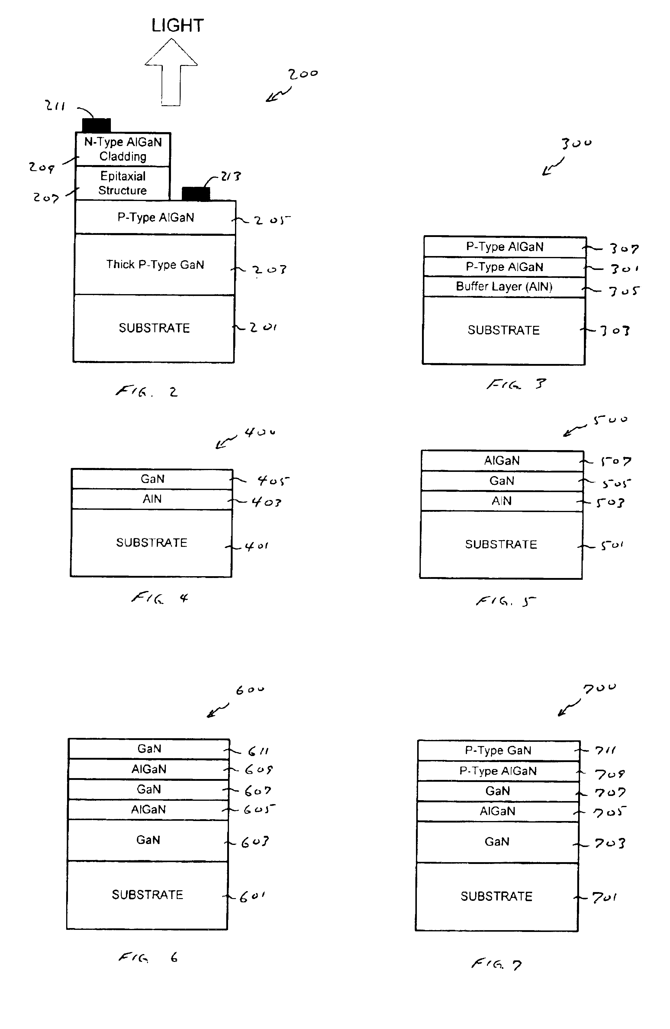
[0050]As illustrated in FIG. 2, a 4 inch sapphire substrate 201 with a (0001) surface orientation was loaded into an HVPE reactor and a 12 micron p-type GaN layer 203 with a Mg concentration of 3×1020 cm−3 was grown following the process described above. After GaN layer 203 was grown, substrate 201 was removed from the growth zone and aluminum trichloride was delivered to the growth zone. Gallium chloride and Mg vapor continued to be delivered to the growth zone. Substrate 201 was then reintroduced into the growth zone and a 0.3 micron thick p-type AlGaN layer 205 with an AlN concentration of 15 molecular percent and an Na—Nd concentration of 5×1019 cm−3 was grown. The substrate was removed from the growth zone after completion of the AlGaN layer. In a separate epitaxial process utilizing an additional source (i.e., indium), an n-type multiple quantum well InGaN structure 207 was grown on top of p-type AlGaN layer 205. After completion of the InGaN structure, an n-type AlGaN claddin...

embodiment iii

[0051]FIG. 3 illustrates another embodiment of the invention. In this embodiment a thick p-type AlGaN layer 301 was grown on a sapphire substrate 303. Layer 301 can be grown without misorientation from the (0001) plane, or with a small misorientation angle preferably in the range of 0 to 3 degrees and more preferably in the range of 0.5 to 3 degrees. The AlN concentration can be set between 0 and 60 molecular percent with an Na—Nd concentration preferably greater than 5×1018 cm−3, and more preferably greater than 1×1019 cm−3.

[0052]Although AlGaN layer 301 can be grown directly on substrate 303, in this embodiment an AlN buffer layer 305, preferably between 0.05 and 0.5 microns thick, is interposed between layer 301 and the substrate. Alternately, buffer layer 305 can be comprised of aluminum oxy nitride. Buffer layer 305 is formed after the substrate has been etched (e.g., treated with HCl and / or gaseous aluminum chloride for 5 to 20 minutes) using HVPE techniques in which layer 305...


PUM

PropertyMeasurementUnit
temperatureaaaaaaaaaa

Abstract

A method for fabricating semiconductor devices with thin (e.g., submicron) and/or thick (e.g., between 1 micron and 100 microns thick) Group III nitride layers during a single epitaxial run is provided, the layers exhibiting sharp layer-to-layer interfaces. According to one aspect, an HVPE reactor is provided that includes one or more gas inlet tubes adjacent to the growth zone, thus allowing fine control of the delivery of reactive gases to the substrate surface. According to another aspect, an HVPE reactor is provided that includes at least one growth zone as well as a growth interruption zone. According to another aspect, an HVPE reactor is provided that includes extended growth sources such as slow growth rate gallium source with a reduced gallium surface area. According to another aspect, an HVPE reactor is provided that includes multiple sources of the same material, for example Mg, which can be used sequentially to prolong a growth cycle.

Description

CROSS-REFERENCES TO RELATED APPLICATIONS[0001]This application claims the benefit of U.S. Provisional Patent Application Ser. No. 60 / 398,176 filed Jul. 24, 2002 and priority from and is a continuation of U.S. patent application Ser. No. 10 / 113,692 filed Mar. 28, 2002 now U.S. Pat. No. 6,660,083 claiming the benefit of U.S. Provisional Patent Application Ser. Nos. 60 / 280,604 filed Mar. 30, 2001 and 60 / 283,743 filed Apr. 13, 2001, and priority from U.S. patent application Ser. No. 10 / 355,426 filed Jan. 31, 2003 which is a continuation-in-part of U.S. patent application Ser. No. 09 / 900,833 filed Jul. 6, 2001, and priority from U.S. patent application Ser. No. 09 / 903,299 filed Jul. 11, 2001 which is a continuation of U.S. patent application Ser. No. 09 / 900,833 filed Jul. 6, 2001, the disclosures of which are incorporated herein by reference for all purposes.FIELD OF THE INVENTION[0002]The present invention relates generally to semiconductor devices and, more particularly, to a method an...

Claims


Application Information

Patent Timeline
Patent Type & Authority Patents(United States)
IPC IPC(8): C30B25/02H01L21/02H01L21/205C30B25/08C30B25/14C30B25/16C30B29/40
CPCC23C16/303C23C16/4488C23C16/45514C30B25/02C30B25/08C30B25/14C30B25/16C30B29/40C30B29/403C30B29/406H01L21/0237H01L21/02458H01L21/02505H01L21/0254H01L21/02576H01L21/02579H01L21/0262H01L21/02631
Inventor DMITRIEV, VLADIMIR A.TSVETKOV, DENIS V.PECHNIKOV, ALEKSEIMELNIK, YURI V.USIKOV, ALEKSANDRKOVALENKOV, OLEG
Owner OSTENDO TECH INC
Why Eureka
Try Eureka