Method for producing large area antireflective microtextured surfaces

a micro-textured surface and large-area technology, applied in the field of anti-reflective micro-textured surfaces, can solve the problems that the photomask has so far been overlooked, and achieve the effects of excellent anti-reflective properties, easy replication, and good control of the microscopic details of the surface profil

Inactive Publication Date: 2005-10-25
KHUSNATDINOV NIYAZ +1
View PDF12 Cites 151 Cited by
  • Summary
  • Abstract
  • Description
  • Claims
  • Application Information

AI Technical Summary

Benefits of technology

[0013]The object of this invention is to provide a method for forming antireflective microtextured surfaces that involve exposing a photosensitive material with UV radiation through a photolithography mask, or in short ‘photomask’. The photomask can be a binary screen mask, a phase shift mask, or their combination. The key inventive concept is the use of the photomask to spatially modulate the intensity of the UV radiation. Photomasks have been used extensively in the semiconductor industry to write microelectronic circuits of ever decreasing physical dimension. However, the photomask has thus far been overlooked regarding the fabrication of antireflective microtextures that are effective for visible light. In accordance with the object of this invention, it is shown that the photomask is a tool well suited for the fabrication of a specific class of surface relief profiles that possess excellent antireflective properties and also ease of replication.
[0014]The use of the photomask allows good control over the microscopic details of the surface profile since the light intensity distribution depends precisely on the optical properties of the photomask apertures and phase shifters. Further, the photomask provides greater freedom in pattern design since the arrangement of apertures and phase shifters are subject to few constraints. Thus, another object of this invention is to provide a method for patterning that, compared to methods in the prior art, allows greater freedom in the specification of the antireflective profile, yet more control over the actual fabrication of the specified rmicrotextured surface.
[0015]It is still another object of this invention to provide a method for creating large-area antireflective microtextured surfaces that are effectively seamless and free of defects. The use of the photomask is particularly suited for scaleup processes that involve step-and-repeat procedures, due to the uniformity and reproducibility of the individual exposure fields that make up the larger pattern. Alternatively, photomasks are routinely manufactured in large-area geometries of high uniformity and quality. Therefore the method of forming large-area surface relief profiles may simply start with procurement of a large-area photomask.
[0016]The method of using a photomask for fabricating large-area microtextures enables the production of high quality surfaces profiles that may be efficiently replicated to produce effective and inexpensive antireflective treatments. Additional objects, features and advantages of the invention will become apparent from a consideration of the included drawings and ensuing detailed description.

Problems solved by technology

However, the photomask has thus far been overlooked regarding the fabrication of antireflective microtextures that are effective for visible light.

Method used


Image

  • Method for producing large area antireflective microtextured surfaces
  • Method for producing large area antireflective microtextured surfaces
  • Method for producing large area antireflective microtextured surfaces

Examples


example 1

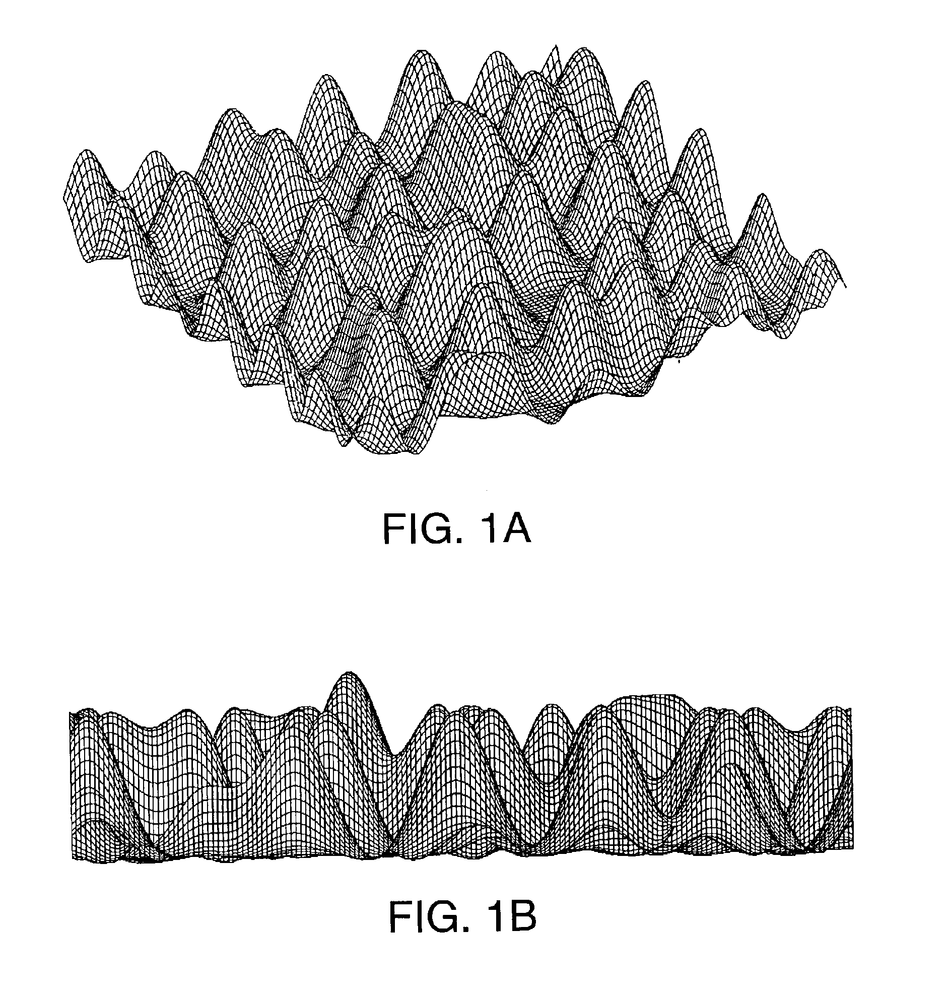
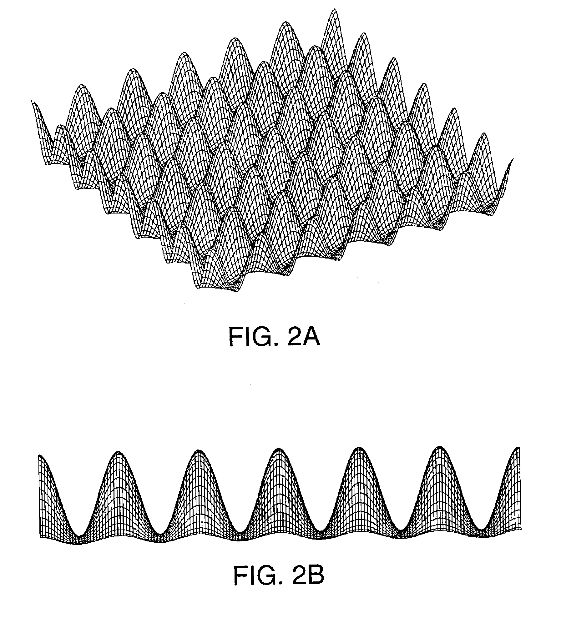
[0045]A typical period of the periodic EAP structure for visible light is 250 nm. By visible light, we mean electromagnetic radiation with wavelength in vacuum in the range from 390 nm to 800 nm. An aligner with NA=0.65 and DUV source wavelength λ=248 nm will give in the image plane Δic=191 nm, fi / fic=0.76, and MTF=0.14. A similar aligner with NA=0.75 gives Δic=165 nm, fi / fic=0.66, and MTF=0.23.

[0046]Special contrast enhancement techniques like oblique off-axis illumination, single-sideband technique, and other aligner specific techniques can significantly increase the value of the modulation transfer function. A phase shift mask, or a binary mask combined with phase shift elements can be employed to increase the contrast of the image as well. Examples of phase shift masks are given below in the context of contact lithography.

[0047]Another way to increase the modulation transfer function is to reduce the exposure wavelength.

example 2

[0048]An aligner with NA=0.65 and DUV light source λ=193 nm gives a critical period in the image plane Δic=148 nm. Thus for the 250 nm period EAP structure, we have fi / fic=0.59, and MTF=0.3 or 30%. That is much better than 14% for the light source with Δ=248 nm (see Example 1).

[0049]Some of the contrast enhancing techniques mentioned above may be combined together to further increase the contrast enhancing effect.

[0050]The photoresist non-linearity, developer concentration and temperature, and developing time can be used to optimize the resulting profile.

Approach II. Contact Lithography

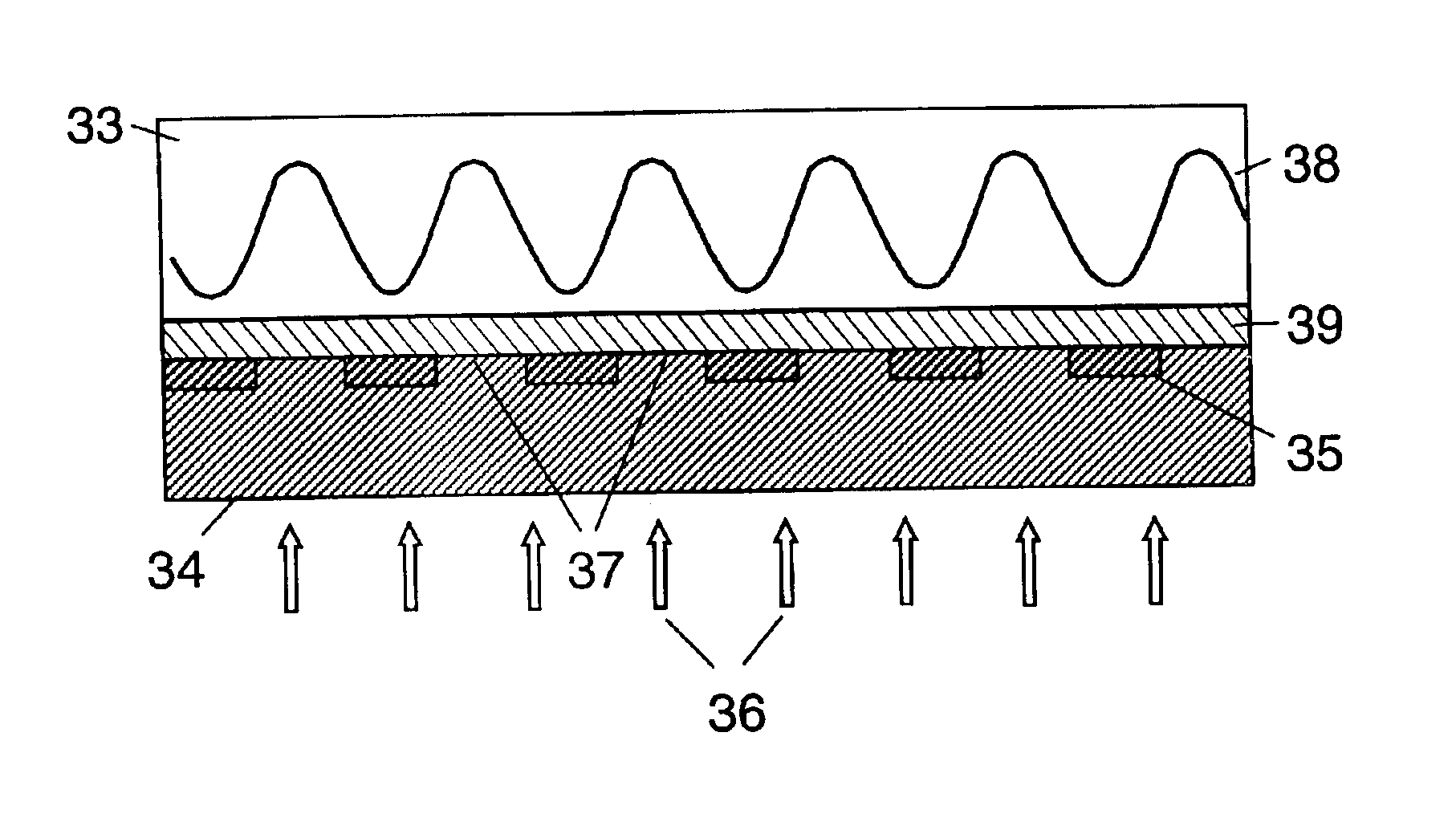
[0051]A subwavelength mask in contact mode can be used with DUV to get the intensity profile of the EAP with a nearest neighbor spacing less than 250 nm. Only light of the zero diffraction order passes through the sub-wavelength aperture. The light has maximum intensity at the center of the aperture provided that incident light is perpendicular to the aperture plane. The intensity of light drops towar...


PUM

PropertyMeasurementUnit
total heightaaaaaaaaaa
distanceaaaaaaaaaa

Abstract

A method employing a photolithography mask for producing microtextured antireflective surfaces is disclosed. The photolithography mask is used during the exposure of photoresist to a pattern of ultraviolet light. The exposed photoresist is subsequently processed to obtain a microtextured surface possessing antireflective properties. The antireflective surface profile comprises an array of sub-micron protuberances that may reside in a periodic arrangement, a quasiperiodic arrangement, or in an arbitrary non-periodic arrangement. The antireflective surface is designed for visible light. It may be scaled-up to large areas, and is suitable for replication into inexpensive polymer materials.

Description

TECHNICAL FIELD[0001]This invention relates to antireflective microtextured surfaces. It further relates to microtextured antireflective polymeric films and resins. The present invention also relates to polymeric films that may be attached, adhered, or otherwise disposed onto optically transparent substrates to enhance their visual properties. Further, the present invention relates to methods for producing surface structures with gradient change of index of refraction. The invention also relates to the fabrication of large area, visually seamless microtextured surfaces.BACKGROUND OF THE INVENTION[0002]A need exists for an antireflective treatment that is characterized by extremely low reflectance and high transmittance over a broad wavelength band, even at high angles of incidence. Additionally, it must be cost effective, flexible, and able to cover large areas. Such a solution would be particularly useful as an easily distributed antireflective treatment that may be applied onto gl...

Claims


Application Information

Patent Timeline
Patent Type & Authority Patents(United States)
IPC IPC(8): G02B5/00G02B1/11G02B5/02G03F1/00G03F7/00G03F7/20
CPCG02B1/11G02B5/0221G02B5/0268G02B5/0278G03F7/0005G03F7/2014G03F1/26
Inventor KHUSNATDINOV, NIYAZCHANG, TANWIN
Owner KHUSNATDINOV NIYAZ
Why Eureka
Try Eureka