Method for manufacturing semiconductor device

a manufacturing method and semiconductor technology, applied in the direction of semiconductor devices, basic electric elements, electrical equipment, etc., can solve the problems of unsuitable mass production, high production cost, and low yield of substrates, and achieve excellent impact resistance properties and high yield

Inactive Publication Date: 2006-08-01
SEMICON ENERGY LAB CO LTD
View PDF18 Cites 84 Cited by
  • Summary
  • Abstract
  • Description
  • Claims
  • Application Information

AI Technical Summary

Benefits of technology

[0009]It is an object of the invention to provide a separation method with high yield without damaging a lamination body. It is another object of the invention to provide a method of manufacturing a lightweight, flexible semiconductor device that is entirely thin.
[0020]According to the invention, separation can be performed at high yield without damaging a lamination body. A semiconductor device having a semiconductor element can be formed on a plastic substrate. As a consequence, a lightweight, thin semiconductor display device with an excellent impact resistance property can be manufactured. In addition, a semiconductor device having a curved surface or a semiconductor device that can be varied in shape can be manufactured.

Problems solved by technology

A glass substrate and a quartz substrate has been typically used for forming the image display device now, however, these substrates have some drawbacks of being fragile and heavy.
Further, these substrates are unsuitable for mass-production since the surface area thereof is difficulty enlarged.
In the case of using the flexible plastic substrate, however, the maximum temperature of the process should be lowered since the plastic film has low heat resistant properties.
This might damage the lamination body.
Accordingly, poor separation might be caused even when laser beam is irradiated to the separation layer, which results in reduced yield.

Method used


Image

  • Method for manufacturing semiconductor device
  • Method for manufacturing semiconductor device
  • Method for manufacturing semiconductor device

Examples


embodiment mode 1

[Embodiment Mode 1]

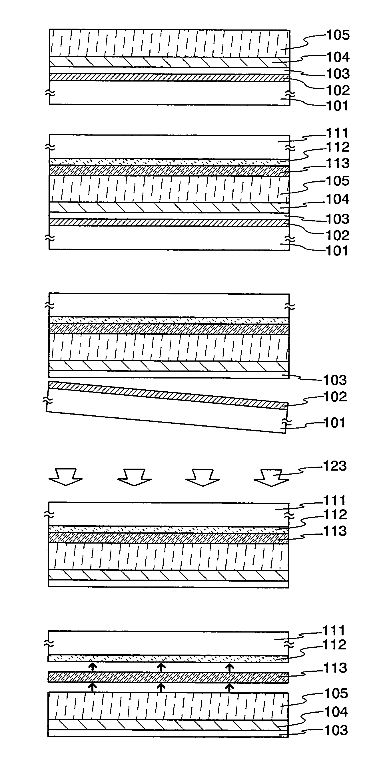
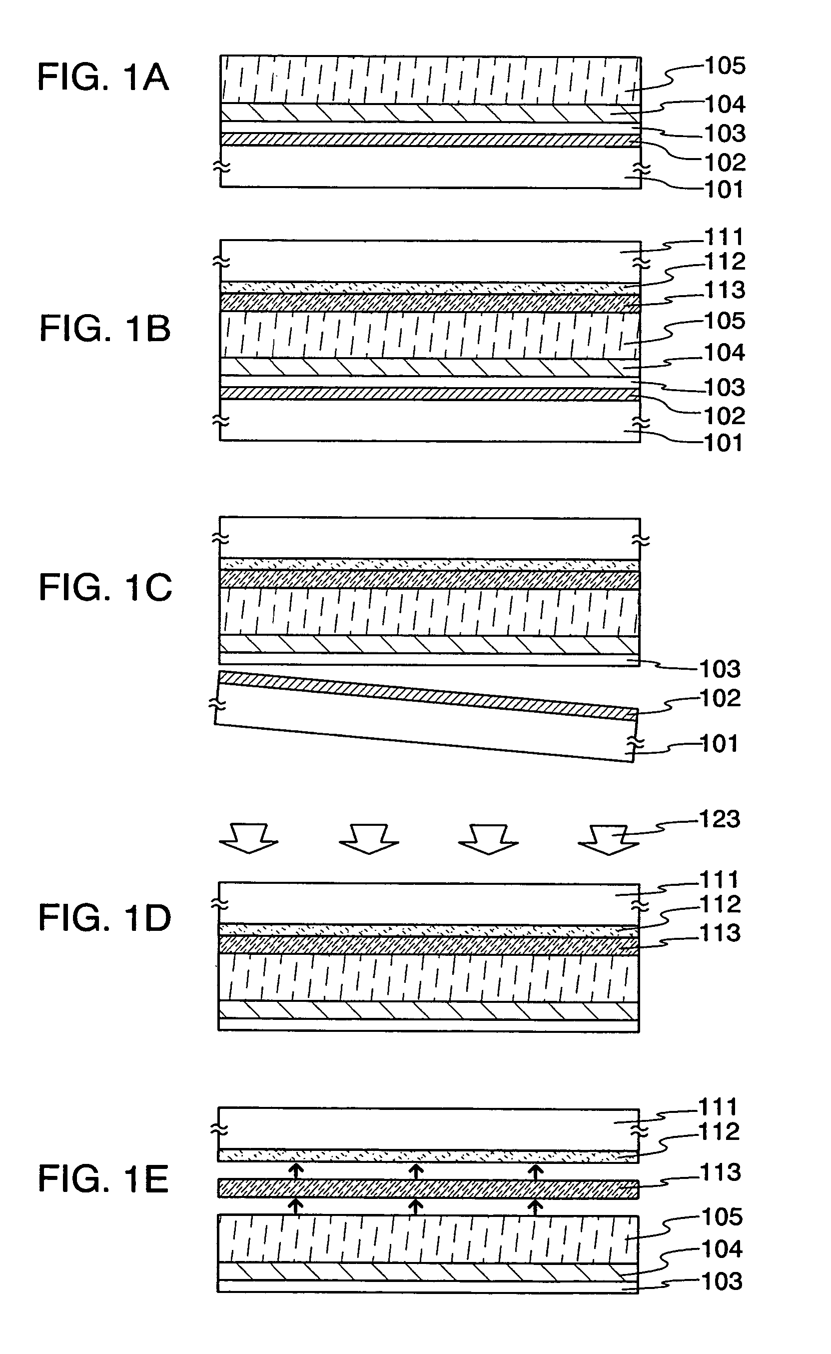
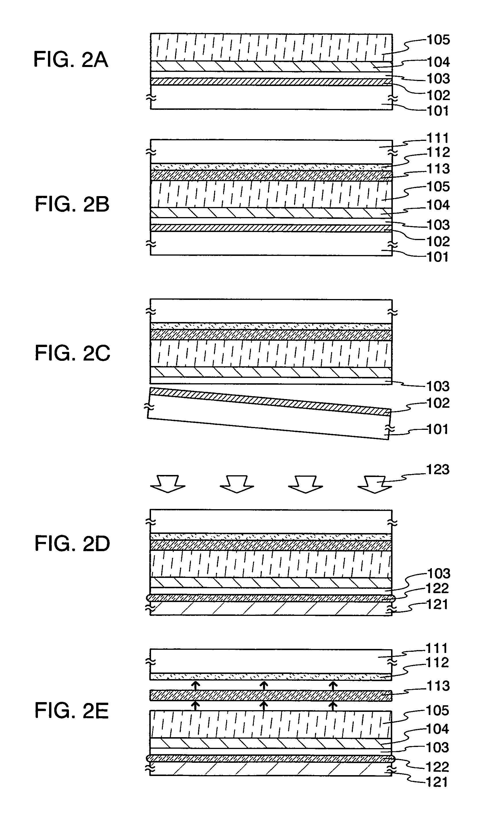
[0041]In the present embodiment mode, a method of separating a lamination body formed over a substrate will be described with reference to FIGS. 1A to 1E.

[0042]As shown in FIG. 1A, a metal film 102 is formed on a first substrate 101. As the first substrate, a heat-resistant substrate, i.e., a material that can withstand the heat treatment in a step of manufacturing an optical filter formed later and the separation step, typically, a glass substrate, a quartz substrate, a ceramic substrate, a silicon substrate, a metal substrate, or a stainless substrate can be used.

[0043]The metal film 102 may be formed of an element selected from titanium (Ti), aluminum (Al), tantalum (Ta), tungsten (W), molybdenum (Mo), copper (Cu), chromium (Cr), neodymium (Nd), iron (Fe), nickel (Ni), cobalt (Co), ruthenium (Ru), rhodium (Rh), palladium (Pd), osmium (Os), iridium (Ir); a single layer formed of an alloy material containing the above-mentioned elements as its main constituent; o...

embodiment 1

[Embodiment 1]

[0064]In the present embodiment, a method of manufacturing a semiconductor device using Embodiment Mode 1 will be described with reference to FIGS. 3A to 3E and FIGS. 4A to 4D.

[0065]As shown in FIG. 3A, a metal film 302 (e.g., a tungsten film with a thickness of 10 to 200 nm, preferably, 30 to 75 nm) is formed on a first substrate 301. The metal film is heated to form an oxide film 303 (e.g., a tungsten oxide film) with a thickness of 1 to 10 nm, preferably, 2 to 5 nm.

[0066]Since the tungsten film and the tungsten oxide film are also formed on edge surfaces of the substrate by sputtering, they are preferably and selectively removed therefrom by O2 ashing etc.

[0067]An anti-reduction film 304 is formed by sputtering. In the embodiment, an AlNxOy film is formed by using an aluminum nitride (AlN) target under an atmosphere of containing a mixture of argon gas, nitrogen gas, and oxygen gas. A first insulating film 305, e.g., a silicon oxynitride film, is next laminated by P...

embodiment mode 2

[Embodiment Mode 2]

[0092]The present embodiment will explain a method of manufacturing a semiconductor device having an inverted-stagger type TFT with reference to FIGS. 5A to 5D, and FIGS. 6A to 6E.

[0093]As shown in FIG. 5A, a metal film 302 with a thickness of 10 to 200 nm, preferably, 30 to 75 nm, an oxide film 303 with a thickness of 1 to 10 nm, preferably, 2 to 5 nm, an anti-reduction film 304, and a base insulating film with a thickness of 100 nm are sequentially laminated on a first substrate 301 in the same manner as Embodiment 1. In the present embodiment, a molybdenum film is formed as the metal film whereas a molybdenum oxide film is formed as the oxide film. As the anti-reduction film, a titanium nitride film having a conductive property is formed.

[0094]Subsequently, gate electrodes 506 and 507 are formed. For example, the gate electrodes may arbitrarily be formed as follows. After forming a conductive film by sputtering, vapor deposition, etc., the conductive film is et...


PUM

PropertyMeasurementUnit
thicknessaaaaaaaaaa
thicknessaaaaaaaaaa
thicknessaaaaaaaaaa

Abstract

A method of separating a lamination body with high yield without damaging the lamination body is provided. Further, a method of manufacturing a lightweight, flexible semiconductor device, which is thin in total is provided. The method of manufacturing the semiconductor device includes: a first step of laminating a metal layer, an oxide layer, a layer containing no hydrogen element, and a lamination body on a first substrate; a second step of forming a photocatalytic layer on a transparent substrate; and a third step of attaching the photocatalytic layer to the surface of the lamination body by using a first adhesive material after the first and second steps, separating the metal layer from the oxide layer, and irradiating light from a side of the transparent substrate so that an interface between the photocatalytic layer and the first adhesive material is separated to remove the first adhesive material.

Description

BACKGROUND OF THE INVENTION[0001]1. Field of the Invention[0002]The present invention relates to a method of separating (or peeling) a lamination body and a method of manufacturing a semiconductor device formed using a plastic substrate.[0003]2. Description of the Related Art[0004]In recent years, a technique of forming a thin film transistor (TFT) using a semiconductor thin film (with a thickness of from approximately several nm to several hundreds nm), which is formed over a substrate with an insulated surface, has been attracting attention. The thin film transistor has been widely applied in various electronic devices such as an IC and a display device. In particular, development related to the thin film transistor as a switching element for an image display device has been carried out hurriedly.[0005]Various applications of such an image display device have been expected, and particularly, application to a portable device has been attracting much attention. A glass substrate and...

Claims


Application Information

Patent Timeline
Patent Type & Authority Patents(United States)
IPC IPC(8): H01L21/46H01L21/30H01L21/20H01L21/762H01L21/77H01L21/84
CPCH01L21/2007H01L21/76251H01L27/1266H01L27/124H01L2224/73265H01L29/41733H01L2221/68363H01L2221/68368H01L2224/48091H01L2224/48465H01L21/2022H01L2224/48227H01L2924/01021H01L2924/01055H01L2924/01068H01L2924/3025H01L2924/07811H01L2224/16225H01L2924/00014H01L2924/00H01L2924/12044H01L2924/181H01L2224/05024H01L2224/05008H01L2224/05001H01L2224/05572H01L24/05H01L2924/00012H01L21/02672
Inventor TAKAYAMA, TORUARAI, YASUYUKISUZUKI, YUKIE
Owner SEMICON ENERGY LAB CO LTD
Why Eureka
Try Eureka