
Resist stripping composition and method of producing semiconductor device using the same

a technology of resist stripping and composition, which is applied in the direction of photomechanical equipment, photosensitive material processing, instruments, etc., can solve the problems of weak or corrosive resistance, reduced yield, and etching action on alumina, so as to suppress the rise of line resistance, reduce the width of interconnects, and reduce the effect of etching action

Inactive Publication Date: 2006-08-08
SONY CORP
View PDF10 Cites 11 Cited by
  • Summary
  • Abstract
  • Description
  • Claims
  • Application Information

AI Technical Summary

Benefits of technology

[0011]The present invention was proposed with the object of eliminating these defects of the prior art. Namely, the present invention has as its object to provide a resist stripping composition capable of reliably removing resist residue or polymer residue produced as a by-product of dry etching and capable of keeping to a minimum damage to the interconnects (corrosion or etching). Further, the present invention has as its object to provide a method of producing a semiconductor device capable of eliminating deterioration of characteristics caused by remainder of resist residue or polymer residue and suppressing a rise of resistance caused by decreased line width of the interconnects.
[0012]The inventors conducted various studies so as to achieve the above objects. As a result, they reached the discovery that by adding a sugar alcohol to a stripper based on a fluorocompound, it is possible to suppress damage to the interconnects (corrosion or etching).
[0015]This etching of the layer including alumina is mainly due to the fluorocompound. In experiments by the inventors, it was learned that by using a composition containing a sugar alcohol, the etching action on alumina is greatly suppressed. Sugar alcohol has the function of an anticorrosive. By using a composition containing a sugar alcohol, the etching rate of alumina at the temperature of use (room temperature) becomes no more than 1.0 nm / min. Therefore, as a result, the decrease in width of interconnects composed of aluminum alloys etc. is prevented and the rise of the line resistance is suppressed.

Problems solved by technology

If the resist residue is not completely stripped off, problems occur such as a reduced yield.
However, with these strippers, various defects are observed such as a low removal power of the resist residue weak or corrosiveness with respect to various types of interconnect materials and insulating films.
In particular, at the present, the above problem is surfacing in aluminum alloy interconnects.
However, aluminum alloy interconnects made finer along with the increasingly high integration of semiconductor integrated circuits are corroded or etched by such a stripper.
Further, such a phenomenon is less frequent with amine-based strippers containing hydroxylamine or strippers based on quaternary ammonium compounds, however, the stripping performance of the resist residue or the polymer residue is insufficient.
Moreover, there is a phenomenon where the etching action of other metals (material burying lower layer contact holes such as tungsten) is accelerated causing electrical short-circuits.
Under these circumstances, application is difficult.
For example, if measuring the line resistance-yield characteristic for micro aluminum alloy interconnects, specifically dense interconnects of line and space dimensions of 0.22 μm / 0.24 μm, it is learned that when using conventional chemicals, it is difficult to suppress the rise of the line resistance and ultimately the desired line resistance-yield characteristic cannot be secured.
Of course, if forming interconnects under milder conditions, the extent of rise in the line resistance does not become a problem even in the prior art and consequently a good yield can be secured, but the more the interconnects are miniaturized, the more conspicuous the above problem becomes.
Further, for example, if measuring the relationship between contact chain resistance and yield by TEG (Test Element Group) in a borderless contact structure where locally dense and long aluminum interconnects and upper aluminum interconnects have a larger area than sparse lower contacts (structure where lower contacts are not covered by upper aluminum interconnects), it has been learned that with the above prior art, the desired rise in the contact chain resistance cannot be secured and in the end the yield cannot be secured.

Method used


Image

  • Resist stripping composition and method of producing semiconductor device using the same
  • Resist stripping composition and method of producing semiconductor device using the same
  • Resist stripping composition and method of producing semiconductor device using the same

Examples


example 1

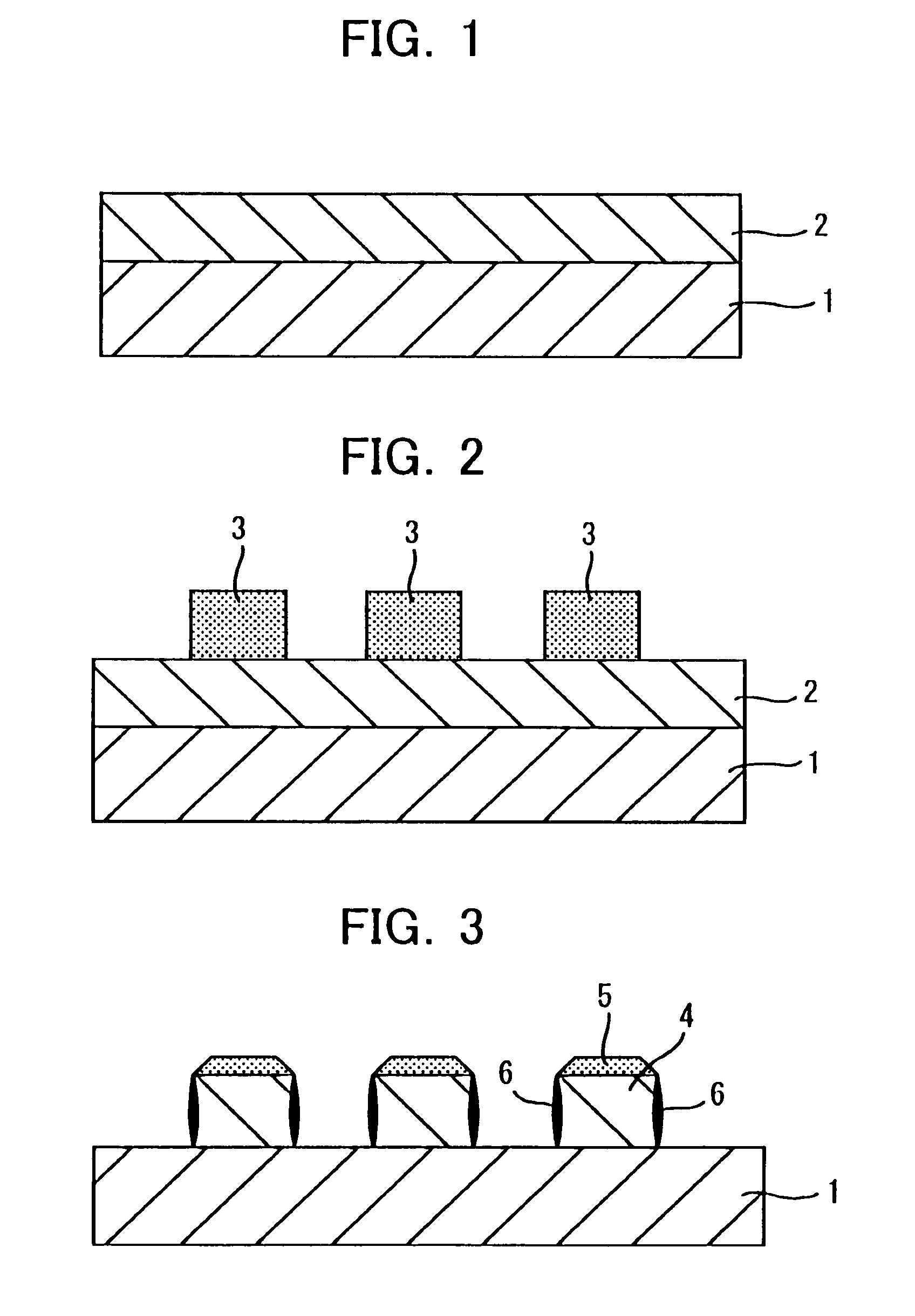
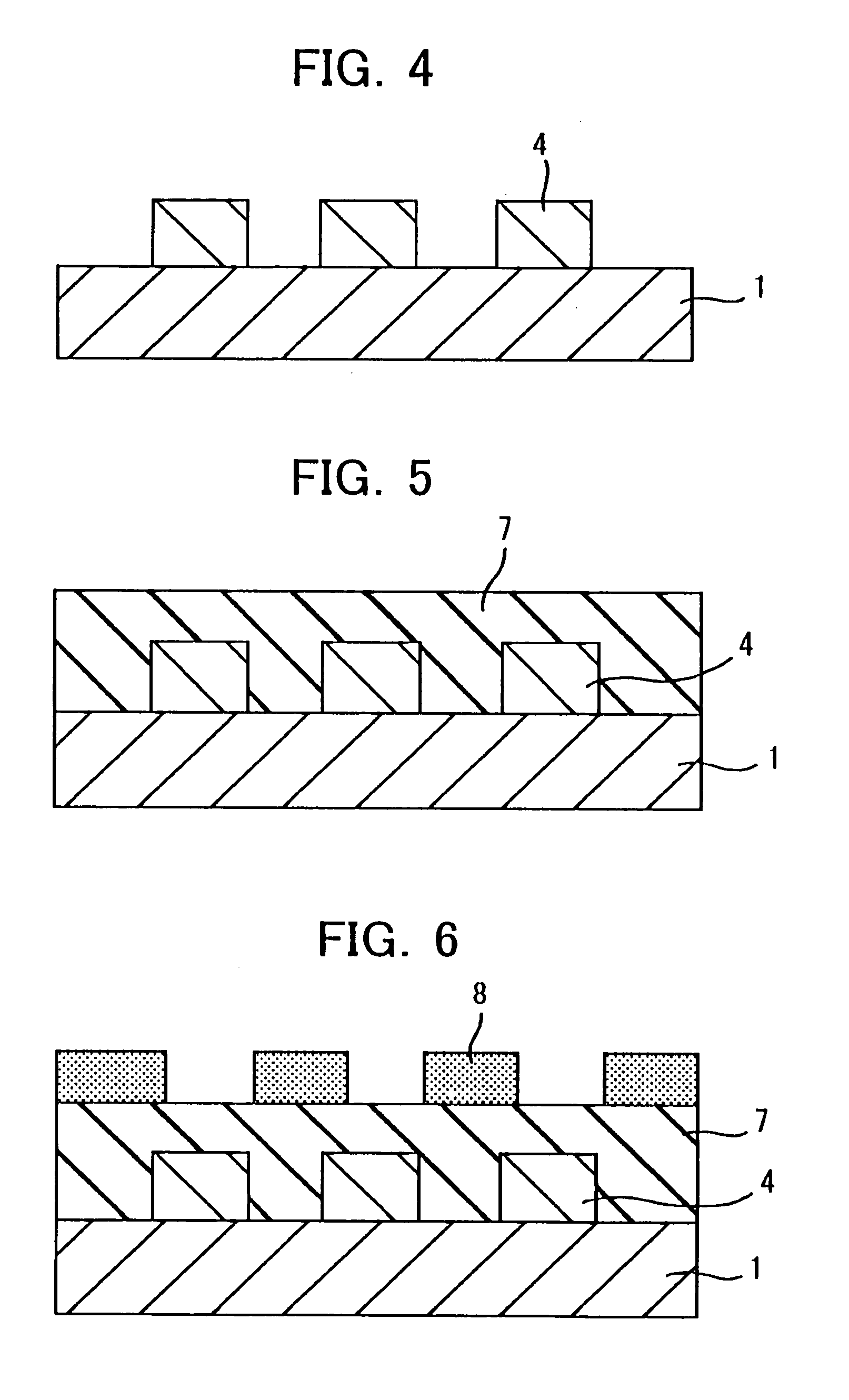
[0047]In the present example, metal interconnects were formed on a base substrate formed in advance with transistors and other devices and the cleaning effect was confirmed. The process of production up to the formation of the first interconnect layer is as follows (see FIG. 1 to FIG. 4).

[0048]Formation of metal interconnect film->dry etching->resist ashing->chemical treatment->pure water rinsing->drying

[0049]The metal interconnect film was made the following five-layer film and was formed by magnetron sputtering.

[0050]Ti 20 nm (0.52 Pa, 2 kW, Ar 35 sccm, 300° C.)

[0051]TiN 20 nm (0.78 Pa, 6 kW, N2 42 sccm, Ar 21 sccm, 300° C.)

[0052]Al-0.5% Cu 500 nm (0.52 Pa, 15 kW, Ar 65 sccm, 300° C.)

[0053]Ti 5 nm (0.52 Pa, 2 kW, Ar 35 sccm, 300° C.)

[0054]TiN 100 nm (0.78 Pa, 6 kW, N2 42 sccm, Ar 21 sccm, 300° C.)

[0055]The dry etching is a step of processing the metal interconnect film to a predetermined pattern. We formed a resist pattern by photolithography and used this as a mask for processing...

example 2

[0103]The composition of the resist stripping composition was changed as follows. Otherwise, the same procedure was followed as in Example 1 to produce a semiconductor device.

[0104]Resist stripping composition:[0105]Ammonium fluoride 0.05 wt %[0106]N,N-dimethylacetamide 40.0 wt %[0107]Diethylene glycol mono-n-butyl ether 51.0 wt %[0108]Xylitol 1.0 wt %[0109]Balance water, pH 8.7

[0110]We measured the line resistance-yield characteristic of the metal interconnects in the semiconductor device produced as explained above. FIG. 12 is a graph showing the relation between line resistance and yield in Example 2 (EXP2) compared with the prior art (PA). The ordinate is the cumulative probability (CP), while the abscissa is the line resistance (LR). We measured the characteristic by dense interconnect TEG of a line and space of 0.22 μm / 0.24 μm. As illustrated, it became possible to suppress a rise in the line resistance compared with the prior art. As a result, it was learned that the desired ...


PUM

PropertyMeasurementUnit
Concentrationaaaaaaaaaa

Abstract

A resist stripping composition capable of reliably stripping off resist residue or polymer residue and keeping damage to the interconnects to a minimum and a method of producing a semiconductor device using the same, where the resist stripping composition comprises a salt of hydrofluoric acid and a base not including a metal, an organic solvent, a sugar alcohol such as xylitol, and water and has a hydrogen ion concentration of at least 8. The method of production of a semiconductor device comprises dry etching a metal layer or a semiconductor layer on a semiconductor substrate to form an interconnect layer having a predetermined pattern or forming an insulation layer on a semiconductor substrate formed with an interconnect layer and dry etching this to a predetermined pattern, then performing chemical treatment using a resist stripping composition comprising a salt of hydrofluoric acid and a base not including a metal, an organic solvent, a sugar alcohol such as xylitol, and water and having a hydrogen ion concentration of at least 8.

Description

[0001]This application claims priority to Japanese Patent Application Number JP2001-370742, filed Dec. 4, 2001, which is incorporated herein by reference.TECHNICAL FIELD[0002]The present invention relates to a resist stripping composition, more particularly to a resist stripping composition preferably used for production of an IC, LSI, or other semiconductor device and a semiconductor device in a liquid crystal display, able to strip the resist at a low temperature in a short time, having a high safety, and easy to handle. Moreover, the present invention relates to a method of producing a semiconductor device capable of suppressing etching action on aluminum interconnects formed on a semiconductor substrate due to chemical treatment.BACKGROUND ART[0003]In an IC, LSI, or other semiconductor device and a semiconductor device in a liquid crystal display, aluminum, aluminum alloy, or another conductive metal and SiO2 or other insulating film are formed on a silicon substrate or glass su...

Claims


Application Information

Patent Timeline
IPC IPC(8): C11D7/50G03F7/42H01L21/027H01L21/306H01L21/768
CPCG03F7/422G03F7/423H01L21/76802G03F7/425H01L21/02052G03F7/42
Inventor IWAMOTO, HAYATOKANAMURA, RYUICHIENDOU, AISUZUKI, TOMOKOHIRAGA, TOSHITAKA
Owner SONY CORP
Learn More