
Laser irradiation apparatus

a technology of laser irradiation and equipment, which is applied in the direction of manufacturing tools, crystal growth process, gel state, etc., can solve the problems of poor processing efficiency, achieve high crystallinity, improve crystallinity, and facilitate the effect of irradiation

Inactive Publication Date: 2006-09-12
SEMICON ENERGY LAB CO LTD
View PDF45 Cites 46 Cited by
  • Summary
  • Abstract
  • Description
  • Claims
  • Application Information

AI Technical Summary

Benefits of technology

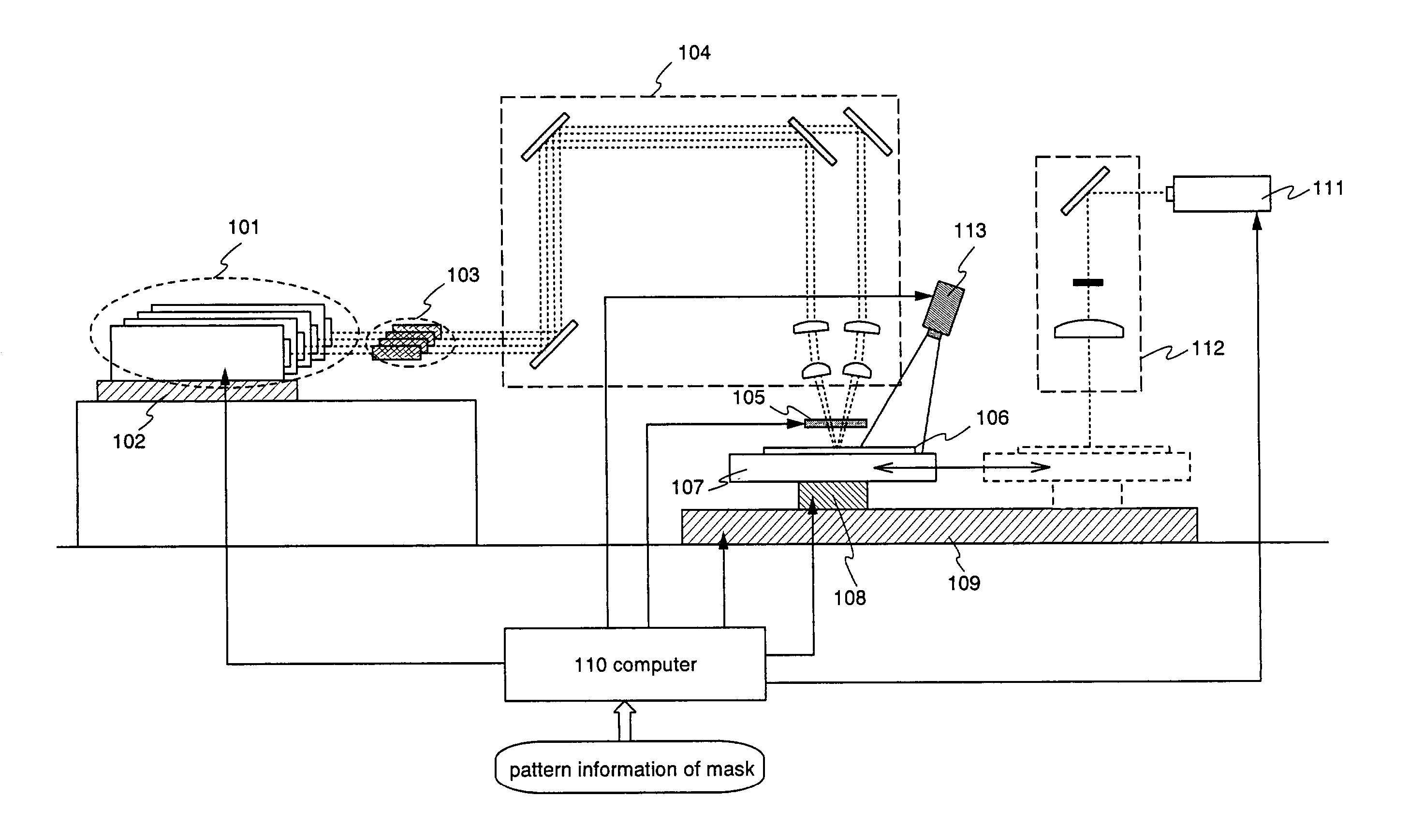
[0014]The present invention has been made in view of the above problems, and therefore it is an object of the present invention to provide a laser irradiation equipment using the laser crystallizing method, which can enhance a processing efficiency of a substrate and the mobility of a semiconductor film in comparison with the conventional example.
[0016]It should be noted here that it does not matter whether the region that has been determined in accordance with the pattern information and should be crystallized is a region of a semiconductor film that will be obtained through patterning after the crystallization or a region thereof that will become the channel formation region of a TFT. In the present invention, the fourth means grasps the region that should be crystallized, determines the scanning path of the laser lights so that the laser lights are scanned onto at least the region that should be crystallized, and controls the third means so that the beam spot moves in accordance with the scanning path. That is, in the present invention, the laser lights are not irradiated onto the entire surface of the semiconductor film but are scanned so that at least each indispensable portion is crystallized to a minimum. With the construction described above, it becomes possible to save a time taken to irradiate the laser lights onto each portion to be removed through patterning after the crystallization of the semiconductor film.
[0017]As described above, in the present invention, the laser lights are not scanned and irradiated onto the entire surface of the semiconductor film but are scanned so that at least each indispensable portion is crystallized, which makes it possible to save a time taken to irradiate the laser lights onto each portion to be removed through the patterning after the crystallization of the semiconductor film. As a result, it becomes possible to shorten a time taken to irradiate the laser lights and also to improve the speed at which a substrate is processed.
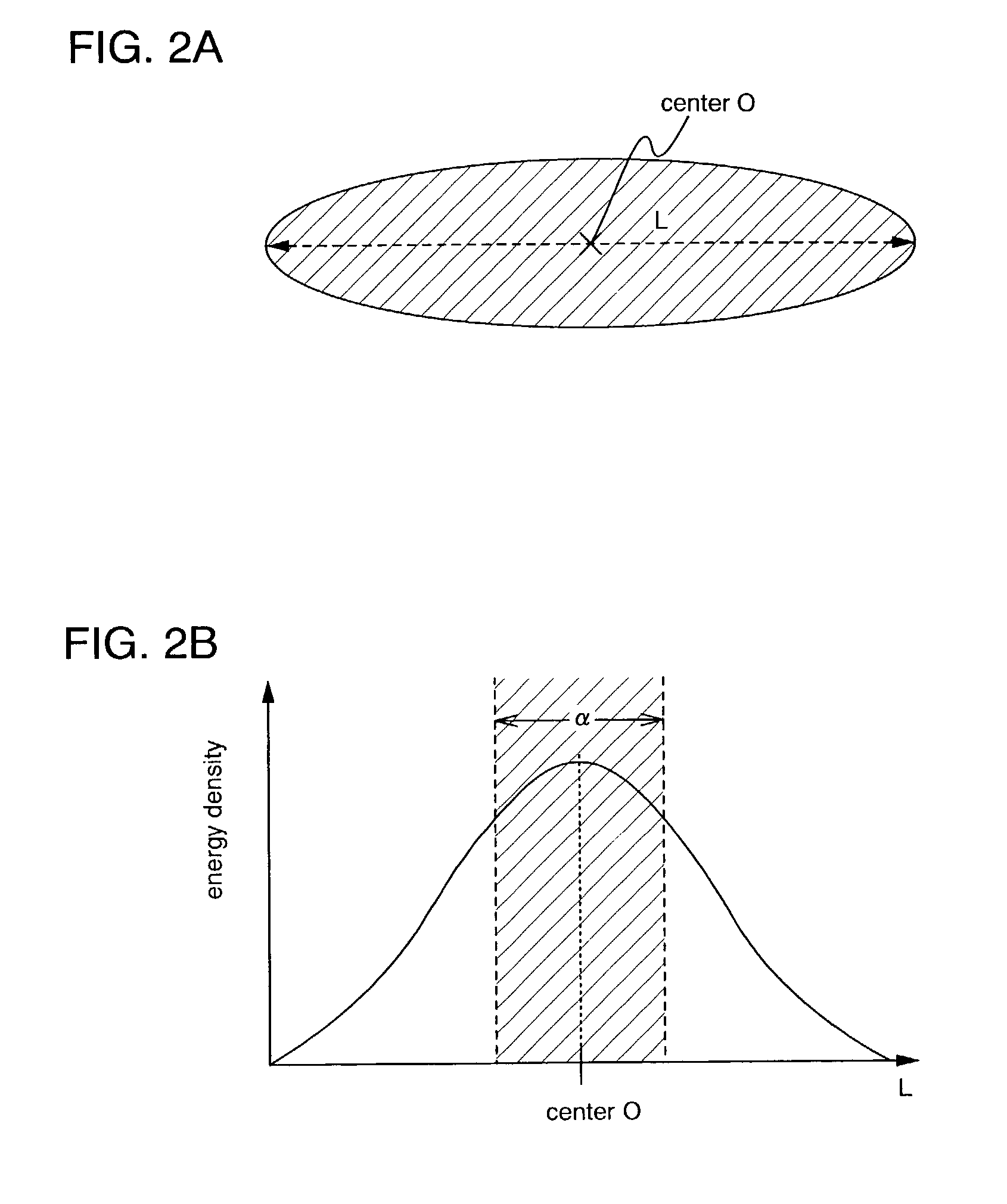
[0018]Also, by synthesizing the laser lights oscillated from the plurality of laser oscillation apparatuses, it becomes possible to have the laser lights complement each other in each portion having a low energy density. Further, by performing the laser light irradiation through the slit, it becomes possible to shield each portion, which has a low energy density, of the beam spot obtained as a result of the synthesizing. As a result, it becomes possible to irradiate laser light, whose energy density is relatively uniform, onto the semiconductor film and to uniformly perform the crystallization. Also, by providing the slit, it becomes possible to partially change the width of the beam spot in accordance with the pattern information and to reduce limitations imposed on the layout of active layers of TFTs. Note that, the width of a beam spot refers to the length of the beam spot in a direction vertical to a scanning direction.
[0021]With the construction described above, some crystal grains obtained by the first laser light irradiation operation are converted into a single larger crystal grain by the second laser light irradiation operation whose scanning direction has been changed. This may be because the crystal grains that have grown in a specific direction during the first laser light irradiation operation function as seed crystals and crystal growing is performed during the second laser light irradiation operation in a direction that differs from the specific direction. As a result, a semiconductor film that has high crystallinity in part is obtained through the laser light irradiation performed twice while changing the scanning direction. Therefore, by producing the active layers of TFTs using the regions, whose crystallinity has been further enhanced, of the semiconductor film, it becomes possible to obtain TFTs having high mobility.
[0022]Also, after the formation of the semiconductor film, the irradiation of the laser lights for crystallizing the semiconductor film may be performed under a state where the exposure to the atmosphere is prevented (for instance, the laser light irradiation is performed under a specific gas atmosphere (such as a rare gas atmosphere, a nitrogen atmosphere, or an oxygen atmosphere) or under a reduced pressure atmosphere). With this construction, it becomes possible to prevent the mixing of a contaminant (boron contained in a filter used to enhance the cleanness of the air, for instance) at a molecule level within a clean room into the semiconductor film during the crystallization using the laser lights.

Problems solved by technology

Thus, processing efficiency is poor and it is an important object to improve the processing speed of the substrate.

Method used


Image

  • Laser irradiation apparatus
  • Laser irradiation apparatus
  • Laser irradiation apparatus

Examples


embodiment 1

[Embodiment 1]

[0159]The crystalline semiconductor film formed by irradiation of laser light comprises aggregations of a plurality of crystal grains. The crystal grains have random positions and sizes and hence, it is difficult to form a crystalline semiconductor film with specified position and size of crystal grains. Accordingly, the active layers formed by patterning the crystalline semiconductor film into the islands may contain grain interfaces (grain boundaries).

[0160]Unlike crystal grains, the grain boundaries contains therein an infinite number of recombination centers and trapping centers associated with amorphous structure and crystal defects. It is known that carriers trapped in the trapping centers increase the potential of the grain boundaries, which form barriers against carriers, so that the carriers are reduced in current transportability. Therefore, the grain boundaries present in the active layer of a TFT, or particularly in the channel forming region, will exert se...

embodiment 2

[Embodiment 2]

[0191]In this embodiment, description is made on an optical system for overlapping beam spot.

[0192]FIGS. 21A and 21B illustrate exemplary optical systems according to the embodiment. FIG. 21A shows a side view an optical system of the laser irradiation equipment of the present invention. FIG. 21B shows a side view that is viewed along the direction of the arrow B in the FIG. 21A. FIG. 21A shows a side view that is viewed along the direction of the arrow A in FIG. 21B.

[0193]FIG. 21 shows an optical system which is adopted synthesize the four beam spots into a single beam spot. In this embodiment, the number of beam spot for synthesizing is not limited to this, the number may range between 2 and 8 (inclusive).

[0194]Reference numerals 401 to 405 are cylindrical lenses, not shown in FIG. 21. The optical system of this embodiment includes six cylindrical lenses. Reference numeral 410 is a slit. FIG. 22 shows a vertical view of optical system shown in FIG. 21. Laser beam pas...

embodiment 3

[Embodiment 3]

[0213]In this embodiment, description is made on an example where the size of the laser beam spots is changed by changing the length of the slit in the course of laser irradiation using a plurality of laser oscillators.

[0214]The laser irradiation equipment provided at the semiconductor fabricating apparatus of the invention is arranged such that the computer determines an area to be scanned with the laser light based on the mask information inputted to the computer. The embodiment is further adapted to change the length of the beam spot according to the configuration of the mask.

[0215]FIG. 26A shows an exemplary relation between a configuration of a mask used for patterning the semiconductor film and a length of the beam spot in a case where a single laser irradiation process is performed. A reference numeral 560 denotes a configuration of the mask used for patterning the semiconductor film. After crystallization by the laser irradiation, the semiconductor film is patt...


PUM

PropertyMeasurementUnit
angleaaaaaaaaaa
timeaaaaaaaaaa
timeaaaaaaaaaa

Abstract

Each region, which should be left on a substrate after patterning, of a semiconductor film is grasped in accordance with a mask. Then, each region to be scanned with laser light is determined so that at least the region to be obtained through the patterning is crystallized, and a beam spot is made to hit the region to be scanned, thereby partially crystallizing the semiconductor film. Each portion with low output energy of the beam spot is shielded by a slit. In the present invention, the laser light is not scanned and irradiated onto the entire surface of the semiconductor film but is scanned such that at least each indispensable portion is crystallized to a minimum. With the construction described above, it becomes possible to save time taken to irradiate the laser light onto each portion to be removed through the patterning after the crystallization of the semiconductor film.

Description

BACKGROUND OF THE INVENTION[0001]1. Field of the Invention[0002]The present invention relates to a laser irradiation equipment that crystallize a semiconductor film using laser light and activate after an ion implantation.[0003]2. Description of the Related Art[0004]In recent years, a technique of forming a TFT on a substrate has greatly progressed, and its application and development for active matrix semiconductor display device has been advanced. In particular, since a TFT using a polycrystalline semiconductor film has higher field-effect mobility than a TFT using a conventional amorphous silicon film, it enables high speed operation. Therefore, although the pixel is conventionally controlled on a driving circuit provided outside the substrate, it is possible to control the pixel on the driving circuit formed on the same substrate.[0005]Incidentally, as the substrate used in the semiconductor device, a glass substrate is expected hopefully as the substrate in comparison with a si...

Claims


Application Information

Patent Timeline
Patent Type & Authority Patents(United States)
IPC IPC(8): C30B1/02H01L21/20H01L21/268H01L21/336H01L21/768H01L21/77H01L27/32H01L29/786H01L51/52
CPCB23K26/0604B23K26/0656B23K26/0738H01L21/76894H01L27/1285H01L27/1296B23K26/0608Y10T117/1004H01L21/2026H01L27/3246H01L27/3258H01L27/3262H01L51/5284Y10T117/1008Y10T117/10B23K26/066H01L21/0242H01L21/02683H01L21/02691H01L21/02381H01L21/02502H01L21/02532H01L21/02686H01L21/02425H01L21/02488H01L21/02422H01L21/02678H01L21/02672H10K59/124H10K59/1213H10K59/122H10K59/8792H10K50/865
Inventor YAMAZAKI, SHUNPEIOHTANI, HISASHIHIROKI, MASAAKITANAKA, KOICHIROSHIGA, AIKOMURAKAMI, SATOSHIAKIBA, MAI
Owner SEMICON ENERGY LAB CO LTD
Learn More