Eureka AIR delivers breakthrough ideas for toughest innovation challenges, trusted by R&D personnel around the world.

Composite particle for dielectrics, ultramicroparticulate composite resin particle, composition for forming dielectrics and use thereof

a technology of composite resin and dielectric, which is applied in the direction of inorganic insulators, pigment treatment with non-polymer organic compounds, conductive materials, etc., can solve the problems of affecting the reliability and endurance of semiconductor boards, affecting the performance of semiconductor boards, etc., and achieves small dielectric loss tangent and high permittivity.

Inactive Publication Date: 2007-01-30
JSR CORPORATIOON
View PDF41 Cites 32 Cited by
  • Summary
  • Abstract
  • Description
  • Claims
  • Application Information

AI Technical Summary

Benefits of technology

[0025]The inventors have made vigorous studies to solve the above described Problem 1, and found that a dielectric capable of being baked at a low temperature of 500° C. or lower and having high permittivity and small dielectric loss tangent can be formed, by using a dielectric-forming composition constituted of particles coated with a conductive metal or an organic compound in part or all the surfaces, and a resin component leading to completion of the present invention (Invention 1).
[0027]In addition, the inventors have made vigorous studies to solve the above described Problem 2, and found that a dielectric capable of being baked at a low temperature of 500° C. or lower, having high permittivity and small dielectric loss tangent, and having a pattern of higher dimensional accuracy can be formed by using a dielectric-forming composition having a specific resin as the resin component in Invention 1, leading to completion of the present invention (Invention 3).
[0029]In addition, as a result of making vigorous studies to solve the above Problem 1, the inventors have found that by using a dielectric-forming composition containing (i) ultrafine particle-resin composite particles constituted of inorganic ultrafine particles of specific sizes and a specific resin component, and (ii) inorganic particles or inorganic composite particles with a conductive metal in which an organic compound or the like is deposited on part or all of the surfaces of the inorganic particles, a dielectric capable of being baked at a low temperature of 500° C. or lower, and having high permittivity and small dielectric loss tangent can be formed, leading to completion of the present invention (Invention 5).

Problems solved by technology

In the conventional methods, however, it has usually been difficult to obtain a layer having high permittivity such as 30 or greater or 50 or greater.
However, this system has a disadvantage that even though the permittivity can be increased, the dielectric loss tangent of the resulting dielectric layer increases, and therefore the amount of heat generated in the dielectric layer in the alternating current electric field increases, which may cause degradation of the multilayer printed-wiring board with a dielectric film provided thereon and the like, and failures such as destruction of joints due to thermal stress, leading to situations in which reliability and endurance of the semiconductor board are likely compromised.
In addition, for example, a composite material of high permittivity containing metal-coated powders of high permittivity and non metal-coated powders of high permittivity is described in Japanese Patent Laid-Open No. 6-84407, but when a composite material with permittivity of 30 or greater is to be obtained, for example, by the method described in the aforementioned publication, the dielectric loss tangent is worsened, thus making it difficult to obtain a composite material having high permittivity and small dielectric loss tangent.
However, there is a disadvantage that this method cannot be applied in the case where the dielectric layer is formed in a situation in which electronic parts are mounted on the wiring board, and thus is incapable of being applied commonly to processes for producing various kinds of semiconductor boards, because baking at a temperature as high as, for example, 1000° C. is required (the problem described hitherto is referred to as “Disadvantage 1”).
In addition, screen printing and the like are known as methods of forming the dielectric layer, but they have a disadvantage that as the board is upsized and fineness of wiring is enhanced, requirement for accuracy of positions of patterns becomes so vigorous that it cannot be satisfied by usual printing (Disadvantage 2).
Therefore, there is a disadvantage that when high frequency signals are transmitted, they are transmitted through only the roughened surface area of the conductive circuit due to the skin effect, and a noise occurs in the signal due to irregularities of the surface.
This disadvantage has been significant especially when the resin substrate having lower permittivity and lower dielectric loss tangent compared to the ceramic board is used.
In addition, the resin substrate has a disadvantage such that it tends to accumulate heat because its heat radiation is poor compared to the conductive board and ceramic board, and consequently the diffusion rate of copper ions constituting the conductive circuit is increased, thereby setting up a migration to cause rupture of the interlayer insulation.
However, in the situation in which it is strongly desired to further reduce the size of the printed-wiring board having the IC mounted thereon for downsizing the entire device such as a cellular phone equipped with the printed-wiring board, the area on which electronic parts such as a resister and condenser other than IC chips is reduced, thus making it increasingly difficult to implement those electronic parts on the printed-wiring board.
Recently, even the semiconductor device containing plastic moldings has come to deal with extremely high-speed signals, and therefore the electric properties of the semiconductor device dealing with such high-speed signals have become controversial.
However, in connection with this conventional wiring board, it is possible to cope with a rise in speed of the signal transmitted and the growth of power noises associated with high-density mounting by enlarging the width of the signal layer and increasing the number of mounted bypass condensers in making a design of wirings, but coping with them in this way results in a problem in which high-density mounting of electronic circuit components on the wiring board cannot be achieved.
In addition, techniques in which the wiring board is coated with a material of high permittivity are disclosed in Japanese Patent Laid-Open No. 5-37161 and Japanese Patent Laid-Open No. 5-160334, but the techniques have a disadvantage that a sufficient condenser capacity cannot be obtained if the area of the wiring board is reduced (Problem 4).

Method used

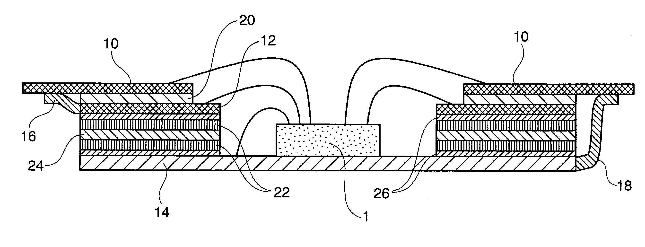
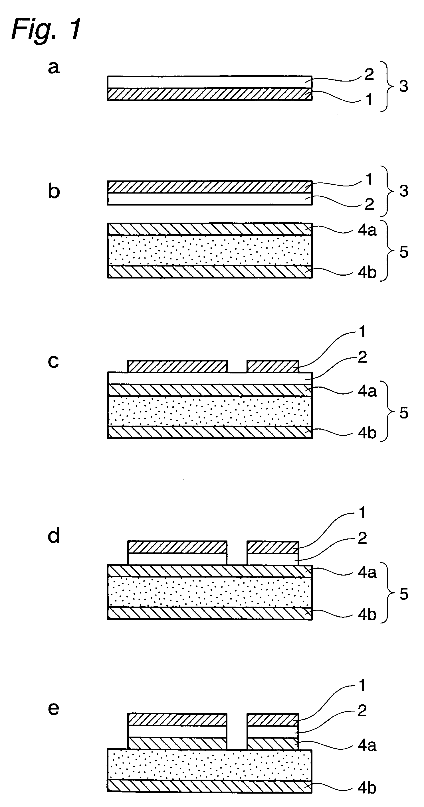
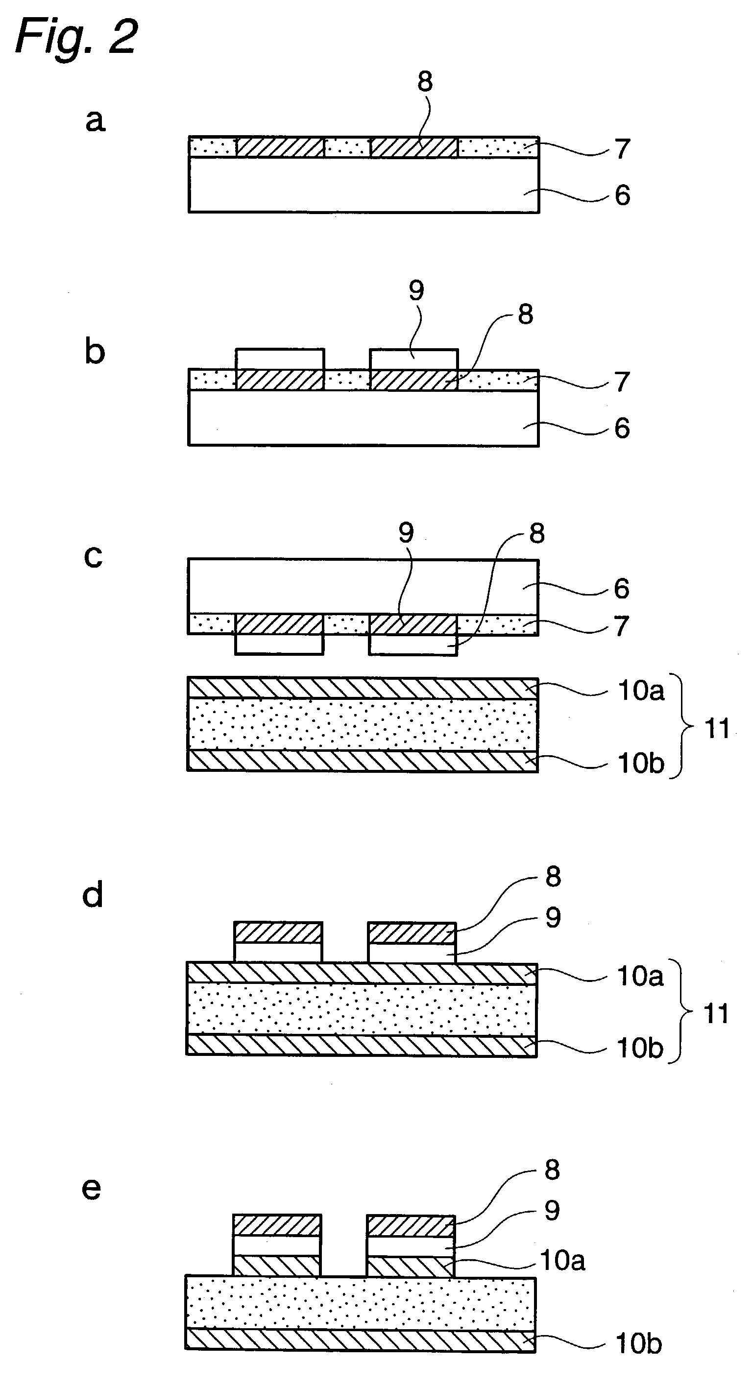

Image

  • Composite particle for dielectrics, ultramicroparticulate composite resin particle, composition for forming dielectrics and use thereof
  • Composite particle for dielectrics, ultramicroparticulate composite resin particle, composition for forming dielectrics and use thereof
  • Composite particle for dielectrics, ultramicroparticulate composite resin particle, composition for forming dielectrics and use thereof

Examples


examples

[0749]The present invention will be described more specifically below using Examples, but the present invention is not limited to these Examples. Furthermore, in the following description, “parts” and “%” are based on weight unless otherwise specified. Also, the weight average molecular weight (Mw) in Examples is polystyrene equivalent average weight measured by gel permeation chromatography (GPC) (trade name: HLC-802A) manufactured by Toso Co., Ltd.

example a

Corresponding to Invention 1

Example A1

Production of Composite Particles for Dielectrics (1)

[0750]Barium titanate particles (trade name: “HPAT-1” manufactured by Fuji Titanium Co., Ltd., average particle size: 0.6 μm, permittivity : 2000) was coated with silver under reduced pressure by the vapor deposition method to obtain composite particles for dielectrics (1) with the surface of barium titanate coated with silver.

[0751]A change in weight before and after the vapor deposition showed that barium titanate had 10% of silver deposited thereon. Also, it was shown from SEM observation of powders that fine particles of silver were deposited on the surfaces of particles.

example a2

Production of Composite Particles for Dielectrics (2)

[0752]100 parts of barium titanate particles (trade name: “AT-02” manufactured by Sakai Chemical Industry Co., Ltd., average particle size: 0.2 μm, permittivity: 2000) and 6 parts of Ketjenblack were preliminarily mixed together, and composite particles for dielectrics (2) with Ketjenblack deposited on the surface of barium titanate were obtained by the mechanochemical method using a hybridizer (Nara Kikai Co., Ltd.).

[0753]It was shown from SEM observation of the resulting powders that fine particles of carbon were deposited on the surfaces of particles. Also, it was shown by SIMS that barium titanate had 5% of carbon deposited on the surface based on the weight ratio.


PUM


Abstract

The dielectric-forming composition according to the invention is characterized by consisting of:composite particles for dielectrics in which part or all of the surfaces of inorganic particles with permittivity of 30 or greater are coated with a conductive metal or a compound thereof, or a conductive organic compound or a conductive inorganic material; and(B) a resin component constituted of at least one of a polymerizable compound and a polymer.In addition, another dielectric-forming composition according to the invention is characterized by containing:ultrafine particle-resin composite particles composed of (J) inorganic ultrafine particles with the average particle size of 0.1 μm or smaller, and (B) a resin component constituted of at least one of a polymerizable compound and a polymer, wherein part or all of the surfaces of the inorganic ultrafine particles (J) are coated with the resin component (B), and the ultrafine particle-resin composite particles contain 20% by weight or more of the inorganic ultrafine particles (J); andinorganic particles with the average particle size of 0.1 to 2 μm and permittivity of 30 or greater, or inorganic composite particles in which a conductive metal or a compound thereof, or a conductive organic compound or a conductive inorganic material is deposited on the part or all of the surfaces of the inorganic particles.

Description

TECHNICAL FIELD[0001]The present invention relates to composite particles for dielectrics, a dielectric-forming composition containing these composite particles for dielectrics, aqueous dispersions for electrodeposition containing this composition, a photosensitive transfer film and dielectric formed of the above described composition and aqueous dispersions for electrodeposition, a dielectrics with a conductive foil (this dielectric formed on the conductive foil), and an electronic part, multilayer circuit board and wiring board comprising this dielectric.[0002]Also, the present invention relates to ultrafine particle-resin composite particles, a dielectric-forming composition containing these ultrafine particle-resin composite particles, aqueous dispersions for electrodeposition containing this composition, a dielectric formed of the above described composition and aqueous dispersions for electrodeposition, a dielectric with a conductive foil (this dielectric formed on the conduct...

Claims


Application Information

Patent Timeline
Patent Type & Authority Patents(United States)
IPC IPC(8): H01B1/22B32B33/00C04B35/00C08K9/02C09C1/36C09C3/06C09C3/08C09D5/00C09D5/44C09D179/08H01B3/00H01B3/12H01G4/20H01L23/14H01L23/495H01L23/498H05K1/03H05K1/16H05K3/00H05K3/46
CPCH01L24/49H01L23/49527H01L23/49589H05K1/0373H05K3/4673C08K9/02H05K1/162H01L23/49894H01L23/145H05K3/0023H05K2201/0257H01L2924/14H01L2924/01058H01L2224/48237H01L2924/01056H01L2924/01079H01L2924/01087H01L2924/014H01L2924/01025H01L2924/0103H01L2924/01083H05K3/4644H01L2924/01014H01L2924/01011H01L2924/01018H01L2224/49109H01L2924/0101H01L2924/01042H01L2924/01023H01L2924/01021H01L2924/01052H01L2924/01013H01L2924/01084H05K2201/0218H01L2924/01019H01L2924/0105H01L2924/01046H01L2924/10253H01L2924/01015H01L24/48H01L2924/04941H01L2924/30105H05K2201/09309H01L2224/48227H01L2924/01039H01L2224/48091H01L2924/01003H01L2924/1517H05K2201/0209H05K2201/0329H01L2924/01006H01L2924/15153H01L2924/01028H01L2924/01044H01L2924/01029H01L2924/01027H01L2924/19041H01L2924/0104H01L2924/01032H01L2924/01016H01L2924/01004H01L2924/01022H01L2924/0102H01L2924/01012H05K2201/0326H01L2924/01038H01L2924/01082H01L2924/01078H01L2924/01007H01L2924/01005H01L2924/01047Y10T428/2998H01L2924/01024H01L2924/01002H05K2201/0355H01L2924/01072H01L2924/01033H01L2924/01074H01L2924/01051H05K2201/0239H05K2203/135H01L2924/00014H01L2924/00H01L2924/351H01L2924/12042H01L2924/12044H01L2224/45099H01B3/00H01B3/10
Inventor ITO, NOBUYUKIMASUKO, HIDEAKIHASEGAWA, SATOMIYOSHIMURA, NAKAATSU
Owner JSR CORPORATIOON
Why Eureka
Eureka Blog
Learn More