Heat treatment apparatus and method of manufacturing a semiconductor device

a heat treatment apparatus and semiconductor technology, applied in the direction of semiconductor devices, semiconductor device details, electrical apparatus, etc., can solve the problems of substrate distortion, cracking, and inability to perform steps, and achieve the effect of increasing reducing the supply amount of coolan

Inactive Publication Date: 2007-02-20
SEMICON ENERGY LAB CO LTD
View PDF46 Cites 11 Cited by
  • Summary
  • Abstract
  • Description
  • Claims
  • Application Information

AI Technical Summary

Benefits of technology

[0009]The present invention has been made to solve the above problems, and an object of the present invention is therefore to provide a technique in which a heating process with high reproducibility can be conducted for a short time
[0011]Further, a coolant introduction port 704 is provided for cooling the semiconductor substrate 707 so that a coolant 705 is introduced into the processing chamber. A coolant exhaust port 706 is provided at one end of the processing chamber 701 so that the coolant 705 is exhausted. An inert gas such as nitrogen, helium, argon, krypton or xenon is used as the coolant 705, and in particular, helium (He) with high thermal conductivity is preferably used. Alternatively, liquid may be used. An inflow of the coolant 705 is adjusted in synchronization with on / off of the light source 702, whereby the temperature rise of the subject substrate itself is prevented. The coolant 705 may be circulated by interposing a means for maintaining a uniform temperature.
[0013]The present invention is characterized in that a cycle of heating by the light source 702 and cooling by circulation of the coolant 705 is repeated plural times. This is called PPTA (plural pulse thermal annealing). In the PPTA, an actual heating time is shortened, and also, light selectively absorbed to the semiconductor substrate is irradiated from a lamp light source. The pulse light shown in FIG. 8 heats the semiconductor substrate, heating is stopped before the heat causes damage to a layer with low heat-resistance, and also, the semiconductor substrate is cooled from the periphery thereof by the coolant, whereby considerable thermal damage is prevented from being caused to the layer with low heat-resistance. Therefore, deformation of the substrate, which has been regarded as a problem in a conventional RTA apparatus, can be prevented.
[0014]Further, the PPTA is conducted under the reduced pressure of 13.3 Pa or less in the processing chamber, whereby oxidization or contamination of the surface of the semiconductor substrate can be prevented. On the other hand, if the PPTA is conducted under the reduced pressure of 13.3 Pa or more, a cooling effect of the semiconductor substrate can be enhanced. Thus, deterioration of the layer with low heat-resistance, such as a wiring formed by using aluminum, can be prevented.
[0015]A turn-on time period per time of lightening by the light source 702 is 0.1 to 60 seconds, preferably 0.1 to 20 seconds, and light from the light source is irradiated plural times. Alternatively, the light from the light source is irradiated in a pulse shape such that a time period for holding the maximum temperature of the semiconductor substrate is 0.5 to 5 seconds. Further, a supply amount of the coolant 705 is increased or decreased with turning-on / turning-off of the light source 702. Thus, heat treatment effect of the semiconductor substrate is enhanced, and also, the thermal damage on the layer with low heat-resistance, which is formed on the semiconductor substrate, is prevented.
[0017]Further, a method of manufacturing a semiconductor device according to the present invention includes a process of heating a semiconductor substrate for a short time, the heating process includes a step of introducing a coolant into a processing chamber in which the semiconductor substrate is placed, and the semiconductor substrate is irradiated with light from a light source plural times with an emission time period per time of lightening by the light source of 0.1 to 20 seconds in the heating process. In the heating process, the coolant is flown through the processing chamber, a supply amount of the coolant is decreased with turning-on of the light source, the light source is turned off, and at the same time, a process of increasing the supply amount of the coolant as one cycle may be repeated plural times. Such a heating process can be conducted after an impurity of one conductivity type is added by an ion injection method.

Problems solved by technology

Thus, the heating process with reproducibility has been difficult to be conducted.
However, since the gate formed of a metal with low heat-resistance is deteriorated, such a step is impossible.
Thus, there has been a problem in that the substrate is distorted and cracked due to thermal stress and other problems.

Method used


Image

  • Heat treatment apparatus and method of manufacturing a semiconductor device
  • Heat treatment apparatus and method of manufacturing a semiconductor device
  • Heat treatment apparatus and method of manufacturing a semiconductor device

Examples


embodiment 1

[0052]An embodiment of a method of conducting a heating process of a semiconductor device by using the heat treatment apparatus of the present invention, which has been described with reference to FIGS. 1 to 6, is described.

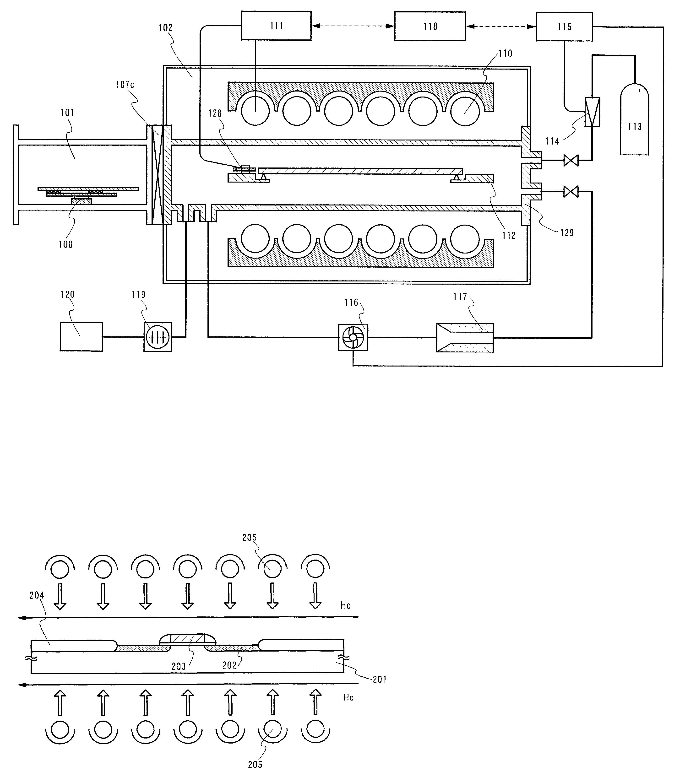
[0053]In FIG. 9, a field oxide film 204, impurity regions 202 formed by ion injection and a gate 203 are formed on a semiconductor substrate 201.

[0054]Here, the heating process for activation of the impurity regions 202 after the ion injection is shown. After the semiconductor substrate is brought into a processing chamber, vacuum exhaust is conducted to approximately 0.1 to 0.0001 Pa by an exhaust means. Then, He as a coolant is introduced. The pressure after the introduction of He is set to approximately 1 to 1000 Pa. Thereafter, as described in FIG. 8, pulse light is irradiated plural times to perform crystallization. The pulse light may be irradiated from one surface or both surfaces of the semiconductor substrate. The impurity regions can be activated to hav...

embodiment 2

[0056]An example of a process of manufacturing a MOS transistor by using a manufacturing device according to the present invention is described.

[0057]In FIGS. 10A to 10C, an n-well 302 and a p-well 303 are formed on a substrate 301 formed of single crystal silicon with relatively high resistance (for example, n type, approximately 10 Ωcm) with one mask in a self-aligning manner. Then, a field oxide film 305 is formed. At this time, boron (B) may be selectively introduced into the semiconductor substrate by an ion injection method to form a channel stopper. Then, a silicon oxide film 306 that becomes a gate insulating film is formed by a thermal oxidization method. Subsequently, a polycrystalline silicon film for a gate is formed with a thickness of 100 to 300 nm by a CVD method. Phosphorous (P) at a concentration of approximately 1021 / cm3 may be previously doped into the polycrystalline silicon film for a gate in order to make resistance lower. Alternatively after the polycrystallin...

embodiment 3

[0066]In this embodiment, an embodiment of a manufacturing process of a MOS transistor using a salicide technique by using the heat treatment apparatus of the present invention is described.

[0067]In FIG. 12A, the same substrate as that in Embodiment 1 is used as a substrate 401, and an n-well 402 and a p-well 403 are formed with one mask in a self-aligning manner. Further, a field oxide film 405 is formed. Then, a silicon oxide film 406 that becomes a gate insulating film is formed by a thermal oxidization method. Gates 407 and 408 are formed of a polycrystalline silicon film added with an n-type impurity typified by phosphorous at a high concentration.

[0068]Next, as shown in FIGS. 12B and 12C, impurity elements respectively imparting an n-type conductivity and a p-type conductivity are added in order to form low concentration drain (LDD) regions in an n-channel MOS transistor and a p-channel MOS transistor. This may be conducted by an ion doping method or an ion injection method. P...


PUM


Abstract

A heat treatment apparatus which enables a heating process for a short time with high reproducibility in a manufacturing process of a MOS transistor manufactured using a semiconductor substrate, and a method of manufacturing a semiconductor device using the heat treatment apparatus are provided. The heat treatment apparatus of the present invention which enables the above heat treatment method is characterized by comprising: a light source; a power supply for turning the light source on and off in a pulse shape; a processing chamber in which the substrate can be irradiated with light from the light source; and a unit for supplying a coolant to the processing chamber and also increasing and decreasing the supply amount.

Description

BACKGROUND OF THE INVENTION[0001]1. Field of the Invention[0002]The present invention relates to a heat treatment apparatus using a rapid thermal annealing (hereinafter referred to as RTA) method, and to a method of manufacturing a semiconductor device using the heat treatment apparatus. In particular, the present invention relates to a heat treatment apparatus that is used in an annealing process conducted for activation after ion injection.[0003]2. Description of the Related Art[0004]In a manufacturing process of a semiconductor integrated circuit, heat treatment is an essential process for the activation of an impurity after ion injection and for the formation of a contact of an electrode. The RTA method is known as a heat treatment technique that is conducted by instantaneously applying heat for several to several tens of seconds. The RTA method is one in which a substrate is rapidly heated mainly using a halogen lamp or the like, and has a characteristic that it is possible to ...

Claims


Application Information

Patent Timeline
Patent Type & Authority Patents(United States)
IPC IPC(8): H01L21/26H01L21/425H01L21/28H01L21/00H01L21/265H01L21/268H01L21/3205H01L21/324H01L21/336H01L21/8238H01L23/52H01L27/092
CPCH01L21/2686H01L21/324H01L21/67115H01L29/665H01L21/823814
Inventor DAIRIKI, KOJIYAMAZAKI, SHUNPEI
Owner SEMICON ENERGY LAB CO LTD
Why Eureka
Try Eureka