Semiconductor element and manufacturing method for the same

a semiconductor element and manufacturing method technology, applied in the field of nitride semiconductor elements, can solve the problems of difficult ohmic contact with the electrode, high contact resistance in the electrode portion, and the problem of emitting element, so as to and increase the light emitting efficiency to the outside

Active Publication Date: 2007-02-27
NICHIA CORP
View PDF6 Cites 90 Cited by
  • Summary
  • Abstract
  • Description
  • Claims
  • Application Information

AI Technical Summary

Benefits of technology

[0014]The present invention is provided in order to solve such problems. A main object of the present invention is to provide a semiconductor light emitting element having a high reflection efficiency, and a manufacturing method for the same, and in particular, to provide a semiconductor light emitting element having a high light emitting efficiency, and a manufacturing method for the same.
[0015]In order to achieve the above described object, a semiconductor element according to the present invention is provided with: a substrate 11 having a pair of main surfaces that face each other; a semiconductor layer of a first conductivity type on one of the main surfaces of the above described substrate 11; a semiconductor layer of a second conductivity type on the above described semiconductor layer of the first conductivity type; an active layer 14 formed between the above described semiconductor layer of the first conductivity type and the above described semiconductor layer of the second conductivity type; and a reflective layer 16 formed on the above described semiconductor layer of the second conductivity type for reflecting light from the above described active layer 14 toward the above described semiconductor layer of the second conductivity type. This semiconductor element can be mounted on a circuit board as a light emitting element, with the other main surface of the above described substrate 11 being used as the main light emitting surface. Furthermore, a translucent conductive layer 17 is formed between the above described reflective layer 16 and the semiconductor layer of the second conductivity type, and an uneven interface 22 is formed as the interface between the above described translucent conductive layer 17 and the above described reflective layer 16. In this configuration, light emitted from active layer 14 to the semiconductor layer of the second conductivity type is reflected from uneven interface 22 so as to be scattered, enhancing the light emitting efficiency to the outside. In particular, unevenness is formed in the interface between translucent conductive layer 17 and the above described reflective layer 16, and therefore, the problem of difficulty in processing the surface of the semiconductor layer of the second conductivity type without deteriorating the properties thereof is solved.
[0016]In addition, the interface between the above described translucent conductive layer 17 and the above described semiconductor layer of the second conductivity type can be made to be an approximately flat and smooth surface in the semiconductor light emitting element. In this configuration, unevenness is formed in the interface between translucent conductive layer 17 and the above described reflective layer 16 without processing the surface of the semiconductor layer of the second conductivity type, so that the light emitting efficiency can be improved.

Problems solved by technology

However, such a nitride-based semiconductor light emitting element has a problem with high contact resistance in the electrode portions.
This is because the band gap of GaN is as wide as 3.4 eV, making ohmic contact with the electrodes difficult.
As a result of this, the contact resistance of the electrode portions becomes high, enhancing the operation voltage of the element, which causes the problem of high consumed power and large amount of heat emission.
On the other hand, light emitting efficiency is also poor.
As a result of this, it is difficult to improve the external quantum efficiency and gain a greater light emitting power.
Also, in the case where a thick p-type GaN layer is formed while doping an impurity with high concentration in order to reduce as much as possible the contact resistance with the electrode, a new problem arises, wherein surface coarseness of the crystal surface occurs.
However, in the case where the surface of a GaN layer is processed so as to be uneven, a problem arises wherein the epitaxial growth layer is damaged in a manner where this portion cannot emit light.
On the other hand, though there is a method where the surface of the p-type GaN layer is made to be flat and the surface of the p-side translucent electrode is processed so as to be uneven, it makes the uneven surface too close to the main light emitting surface, making this uneven pattern visible easily from the outside, and the problem of poor appearance arises.
In addition, in a so-called face-up structure where a p-type electrode is provided on the main light emitting surface, it becomes necessary to provide an n-type electrode, making the main light emitting surface smaller, and in addition, it is necessary for a pad electrode to be provided on the p-type electrode, causing light to be blocked by this portion, which prevents light emission, and the problem of poor light emitting efficiency arises.
However, it is difficult to increase translucency and enhance ohmic properties at the same time, and a further increase in the performance of the conductive oxide film is required.

Method used


Image

  • Semiconductor element and manufacturing method for the same
  • Semiconductor element and manufacturing method for the same
  • Semiconductor element and manufacturing method for the same

Examples


embodiment 1

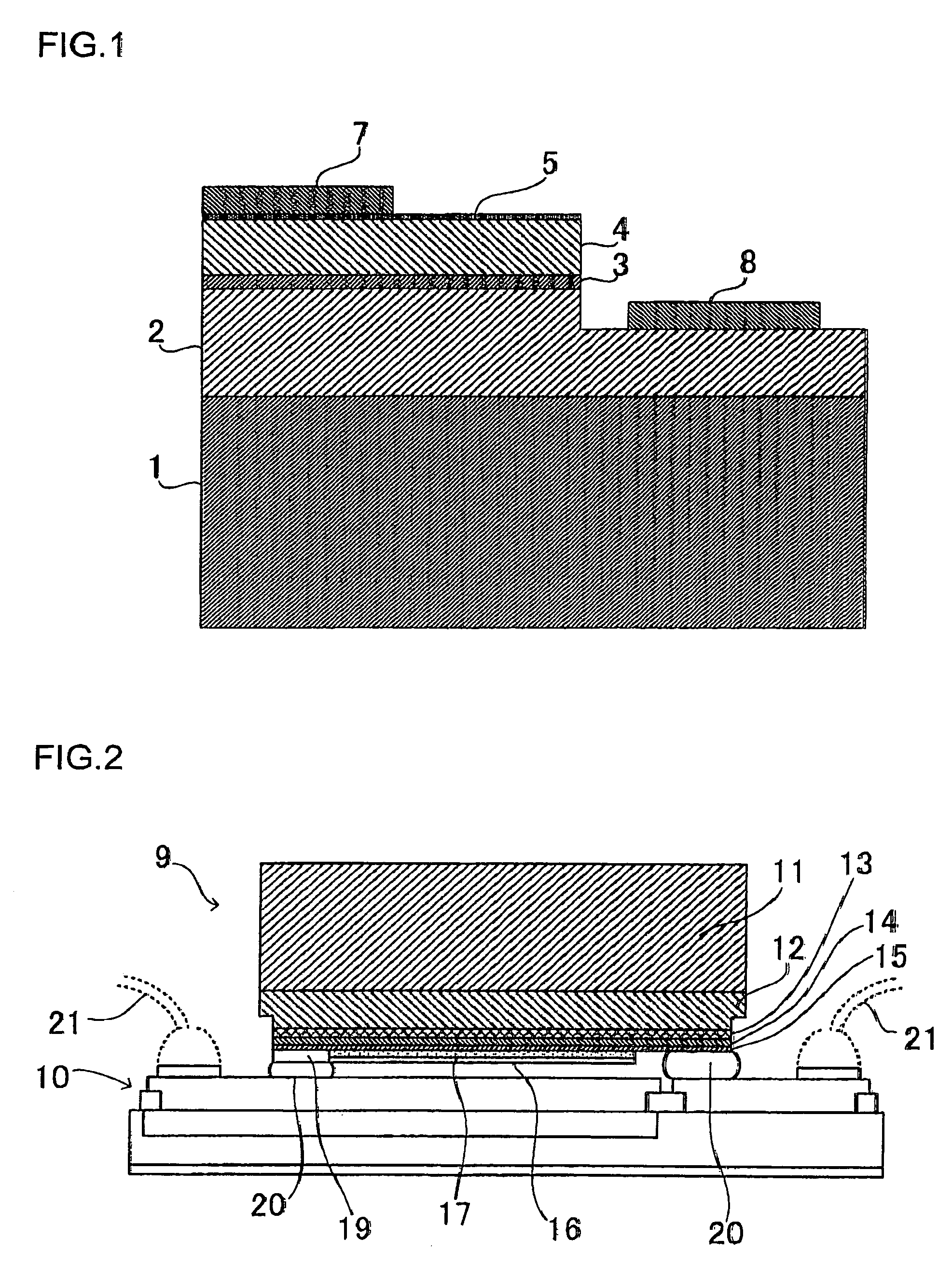
[0045]An example on which a nitride semiconductor light emitting element according to one embodiment of the present invention is mounted is shown in the schematic cross-sectional diagram of FIG. 2. In this figure, an LED chip 9, which is a nitride semiconductor light emitting element, is mounted on a sub-mount 10, which is one type of circuit board, as a flip chip. A flip chip is used in a mounting system, which is referred to as face-down mounting, where the substrate 11 side that faces the surface on which the electrodes are formed is used as the main light emitting surface, unlike face-up mounting, where the surface on which the electrodes of the nitrite semiconductor layer acre formed is used as the main light emitting surface.

[0046]In an LED chip 9 of FIG. 2, a buffer layer 12, an n-type nitride semiconductor layer 13, an active layer 14 and a p-type nitride semiconductor layer 15 are epitaxially grown in sequence on a substrate 11, and furthermore, a translucent conductive lay...

embodiment 2

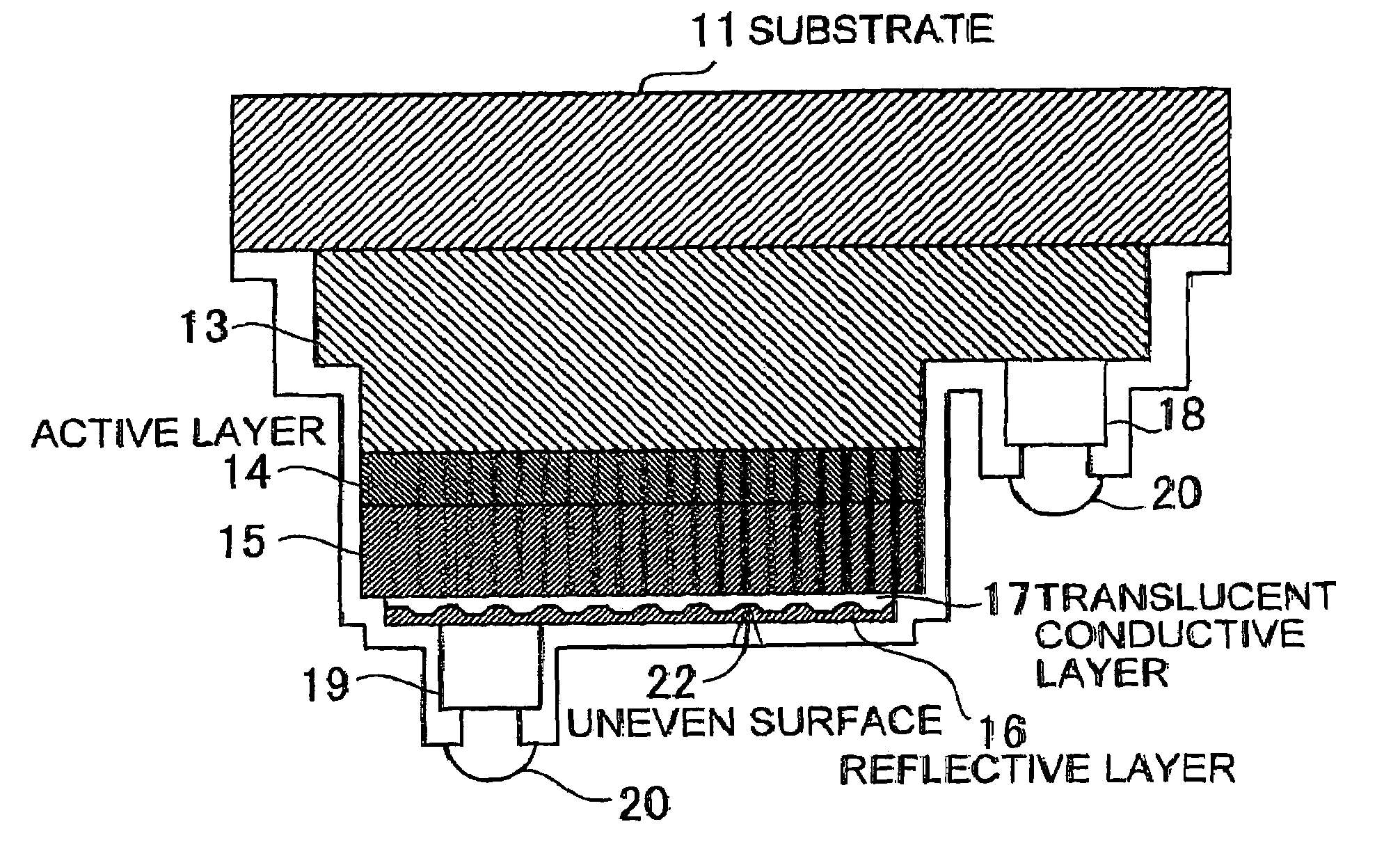
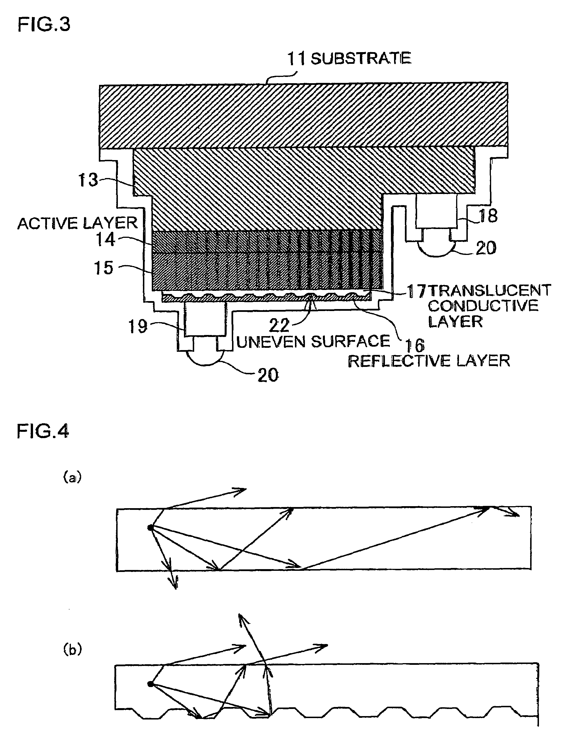
[0101]The semiconductor element according to another embodiment of the present invention is provided with: a substrate 11 which has a pair of main surfaces that face each other; a semiconductor layer of a first conductivity type on one of the main surfaces of the above described substrate 11; a semiconductor layer of a second conductivity type on the above described semiconductor layer of the first conductivity type; an active layer 14 formed between the above described semiconductor layer of the first conductivity type and the semiconductor layer of the second conductivity type; and a reflective layer 16 formed on the above described semiconductor layer of the second conductivity type for reflecting light from the above described active layer 14 toward the above described semiconductor layer of the second conductivity type.

[0102]This semiconductor element can be mounted on a circuit board as a light emitting element, with the other main surface of the above described substrate 11 b...

example 1

[0110]In the following, the examples according to the present invention are described in detail. Here, as Example 1, an LED which is a semiconductor light emitting element having the configuration shown in FIG. 3 is fabricated. First, an MOVPE reactive unit is used and a buffer layer made of GaN is grown in sequence so as to have a film thickness of 200 Angstroms, an n-type contact layer made of an Si doped n-type GaN is grown so as to have a film thickness of 4 μm, an active layer 14 having a single quantum well structure made of non-doped In0.2Ga0.8N so as to have a film thickness of 30 Angstroms, a p-type clad layer made of an Mg doped p-type Al0.1Ga0.9N so as to have a film thickness of 0.2 μm, and a p-type contact layer made of an Mg doped p-type GaN so as to have a film thickness of 0.5 μm, on a sapphire substrate 11 having a diameter of 2 inches.

[0111]Furthermore, annealing is carried out on the wafer in a reactor chamber in a nitrogen atmosphere at a temperature of 600° C., ...


PUM

PropertyMeasurementUnit
angleaaaaaaaaaa
thicknessaaaaaaaaaa
band gapaaaaaaaaaa

Abstract

A nitride semiconductor light emitting element is provided with: a substrate 11 having a pair of main surfaces that face each other; a nitride semiconductor layer of a first conductivity type layered on one of the main surfaces of substrate 11; a nitride semiconductor layer of a second conductivity type layered on the nitride semiconductor layer of the first conductivity type; an active layer 14 formed between the nitride semiconductor layer of the first conductivity type and the nitride semiconductor layer of the second conductivity type; and a reflective layer 16 formed on the nitride semiconductor layer of the second conductivity type for reflecting light from active layer 14 toward the nitride semiconductor layer of the second conductivity type. This nitride semiconductor light emitting element can be mounted on a circuit board, with the other main surface of the above described substrate 11 being used as the main light emitting surface. Furthermore, a translucent conductive layer 17 is formed between reflective layer 16 and the nitride semiconductor layer of the second conductivity type, and an uneven interface 22 is formed as the interface between translucent conductive layer 17 and reflective layer 16.

Description

BACKGROUND OF THE INVENTION[0001]1. Field of the Invention[0002]The present invention relates to a nitride semiconductor element formed of a semiconductor layer where a nitride semiconductor made of AlxInyGa1-x-yN (0≦x, 0≦y, 0≦x+y<1) is layered, and to a manufacturing method for the same, and in particular, to a semiconductor light emitting element such as a light emitting diode (LED) or a laser of which the light emitting efficiency is improved, as well as to a manufacturing method for the same.[0003]2. Description of the Related Art[0004]A light emitting element using a nitride-based semiconductor such as gallium nitride makes light emission of ultraviolet light, blue light, green light and the like possible with high efficiency and low consumed power, and makes miniaturization possible, increasing the strength against mechanical vibration and the like, with the advantage of long lifespan, high reliability and the like, and therefore, is widely applicable to a variety of fields...

Claims


Application Information

Patent Timeline
Patent Type & Authority Patents(United States)
IPC IPC(8): H01L29/22H01L33/06H01L33/10H01L33/22H01L33/32H01L33/42H01L33/58H01L33/62
CPCH01L33/32H01L33/42H01L33/405H01L33/22H01L33/38H01L2933/0091H01L33/46H01L2224/48463
Inventor ICHIHARA, TAKASHISANGA, DAISUKEKUSUSE, TAKESHIYAMADA, TAKAO
Owner NICHIA CORP
Why Eureka
Try Eureka