Semiconductor device and method of manufacturing the same

a semiconductor and semiconductor technology, applied in the manufacture of electrode systems, electric discharge tubes/lamps, instruments, etc., can solve the problems of difficult to manufacture tft having satisfactory performance to meet circuit specifications, unsuitable for use of amorphous semiconductor films, etc., and achieve superior electrical characteristics to tft.

Inactive Publication Date: 2007-03-06
SEMICON ENERGY LAB CO LTD
View PDF88 Cites 24 Cited by
  • Summary
  • Abstract
  • Description
  • Claims
  • Application Information

AI Technical Summary

Benefits of technology

[0009]An object of the present invention is therefore to realize a high performance semiconductor device by manufacturing TFTs each

Problems solved by technology

Since such a driver circuit or a logic circuit is required to perform a high speed operation, it is unsuitable to use an amorphous semiconductor film (typically, an amorphous silicon film) as an active layer.
However, when circuit performance comparable to a conventional IC co

Method used


Image

  • Semiconductor device and method of manufacturing the same
  • Semiconductor device and method of manufacturing the same
  • Semiconductor device and method of manufacturing the same

Examples


embodiment 5

[Embodiment 5]

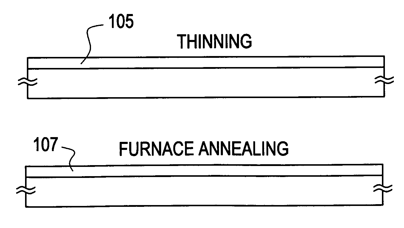
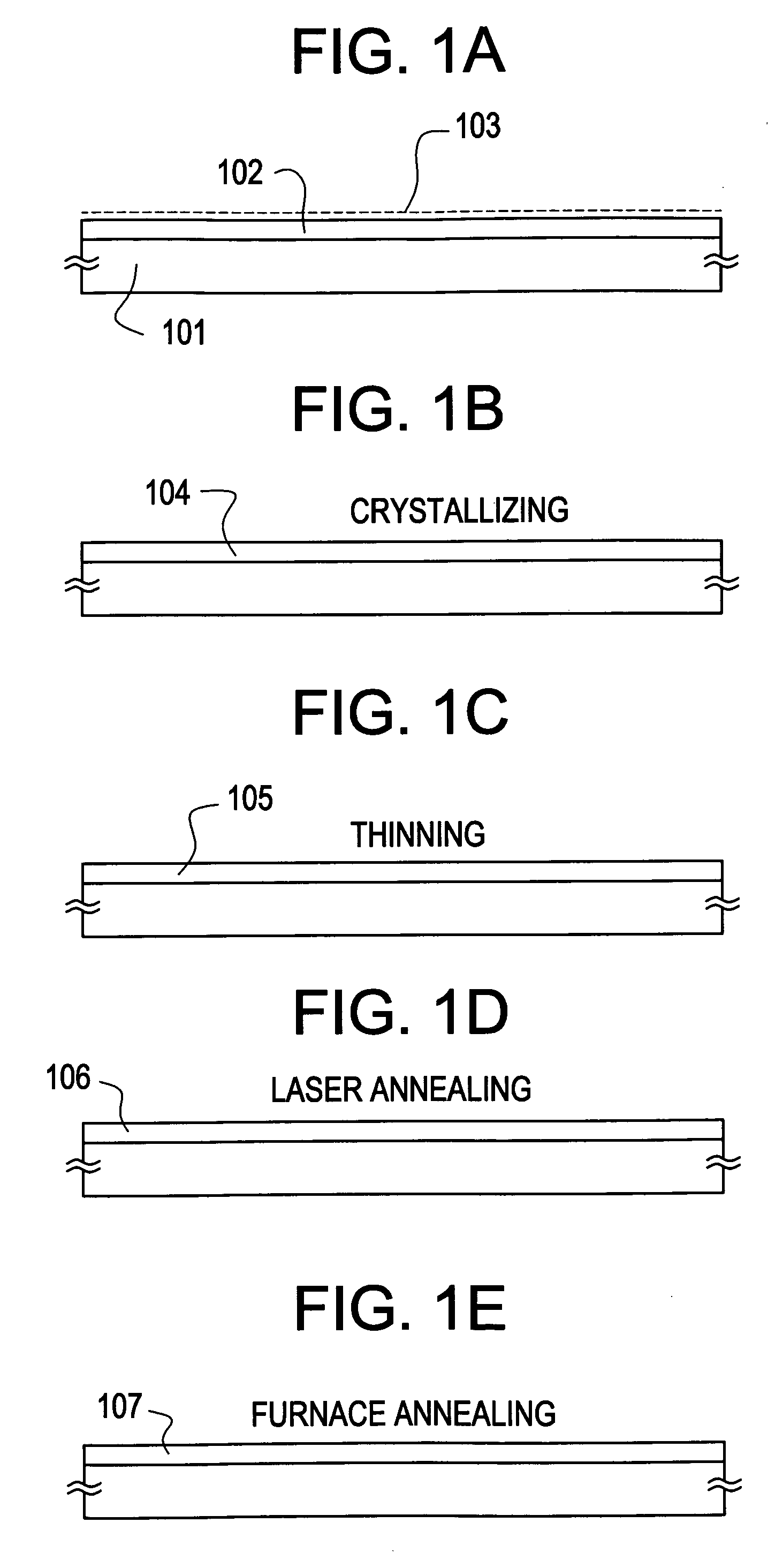
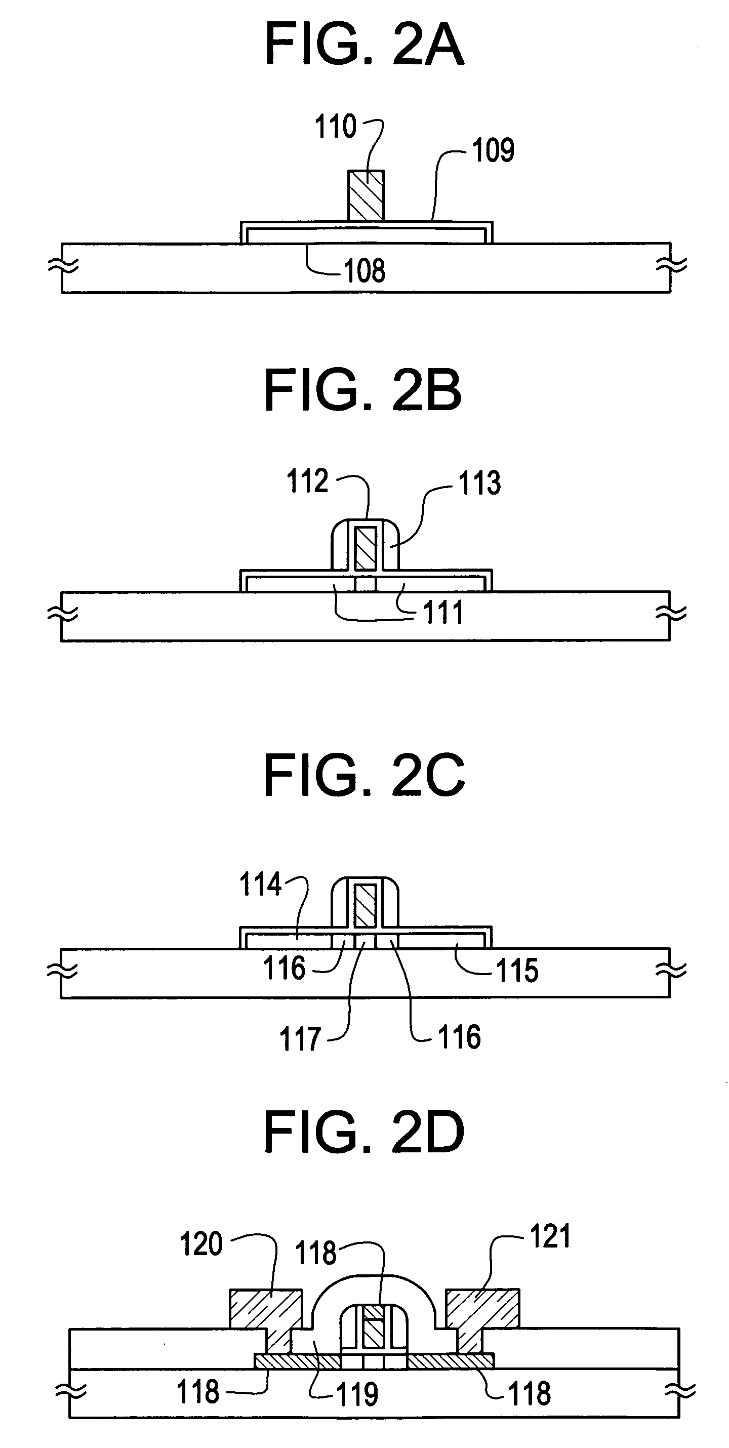
[0172]In this embodiment, steps of manufacturing a TFT on a substrate by carrying out the present invention will be described. FIGS. 5A to 5E are used for the description.

[0173]First, a quartz substrate 1101 was prepared. A material having high heat resistance must be selected as the substrate. Instead of the quartz substrate, a substrate of a material having high heat resistance, such as a silicon substrate, a ceramic substrate, a crystallized glass substrate, or a metal substrate may be used.

[0174]However, although an under film may not be provided in the case where the quartz substrate is used, it is preferable to provide an insulating film as the under film in the case where other materials are used. As an insulating film, it is appropriate that either one of a silicon oxide film (SiOx), a silicon nitride film (SixNy), a silicon oxynitride film (SiOxNy), and an aluminum nitride film (AlxNy), or a laminated film of those is used.

[0175]Besides, it is effective to use...


PUM


Abstract

There is provided a method in which a TFT with superior electrical characteristics is manufactured and a high performance semiconductor device is realized by assembling a circuit with the TFT. The method of manufacturing the semiconductor device includes: a step of forming a crystal-containing semiconductor film by carrying out a thermal annealing to a semiconductor film; a step of carrying out an oxidizing treatment to the crystal-containing semiconductor film; a step of carrying out a laser annealing treatment to the crystal-containing semiconductor film after the oxidizing treatment has been carried out; and a step of carrying out a furnace annealing treatment to the crystal-containing semiconductor film after the laser annealing. The laser annealing treatment is carried out with an energy density of 250 to 5000 mJ/cm2.

Description

BACKGROUND OF THE INVENTION[0001]1. Field of the Invention[0002]The present invention relates to a semiconductor device which includes, as a circuit, a thin film transistor (hereinafter referred to as TFT) using a semiconductor thin film, and a technique regarding a method of manufacturing the same. Incidentally, in the present specification, the semiconductor device means any device which is made to function by using a semiconductor.[0003]Thus, the term “semiconductor device” recited throughout this specification includes not only a single semiconductor component such as a TFT, but also an electro-optical device with TFTs, a semiconductor circuit, and an electronic equipment having those.[0004]2. Description of the Related Art[0005]In recent years, a TFT used for an electro-optical device such as an active matrix type liquid crystal display device has been actively developed. The active matrix type liquid crystal display device is a monolithic display device in which a pixel matrix...

Claims


Application Information

Patent Timeline
IPC IPC(8): H01L21/84G02F1/1362H01L21/20H01L21/268H01L21/336H01L29/786
CPCH01L21/2022H01L21/2026H01L21/268H01L27/1285H01L29/66757H01L29/78675H01L27/1277H01L29/04G02F1/13454H01L21/02686H01L21/02672H01L21/0262H01L21/02532
Inventor OHTANI, HISASHITAKANO, TAMAEYAMAZAKI, SHUNPEI
Owner SEMICON ENERGY LAB CO LTD
Why Eureka
Try Eureka