Semiconductor device and manufacturing method thereof

Inactive Publication Date: 2007-03-13
SEMICON ENERGY LAB CO LTD
View PDF96 Cites 139 Cited by
  • Summary
  • Abstract
  • Description
  • Claims
  • Application Information

AI Technical Summary

Benefits of technology

[0046]According to the present invention, irradiation of a laser beam, heat treatment, or compound treatment of irradiation of a laser beam and heat treatment is performed to a metal layer for performing oxidation treatment, with the result that a metal oxide layer is formed to make it possible to peel a layer to be peeled easily from a substrate with a physical means. In laser irradiation in the oxidation treatment, damage is not caused to a semiconductor layer since the laser irradiation is performed to the metal layer from the substrate side in the case of having no desire to damage the semicondu

Problems solved by technology

However, the substrate used for the previous image display device is a substrate comprising an inorganic material such as a glass substrate or a quartz substrate, as described above, and there are defects of breaking and being heavy, which are unique to the inorganic material.
Compared to the substrate such as the glass or quartz substrate, however, the substrate such as the plastic film has low heat resistance, and therefore, a processing temperature in manufacturing a TFT is limited.
In the result, it was difficult to manufacture a TFT directly on the plastic film, which has favorable characteristics compared to the TFT formed on the glass or quartz substrate.
Consequently, a high-performance image display device or light-emitting device that uses a plastic film has not been realized.
However, since amorphous silicon or polycrystalline silicon is used as the separating layer in the aforementioned method, a problem is considered that an irradiated laser beam is transmitted through the separating layer depending on a film thickness

Method used


Image

  • Semiconductor device and manufacturing method thereof
  • Semiconductor device and manufacturing method thereof
  • Semiconductor device and manufacturing method thereof

Examples


Example

[Embodiment 1]

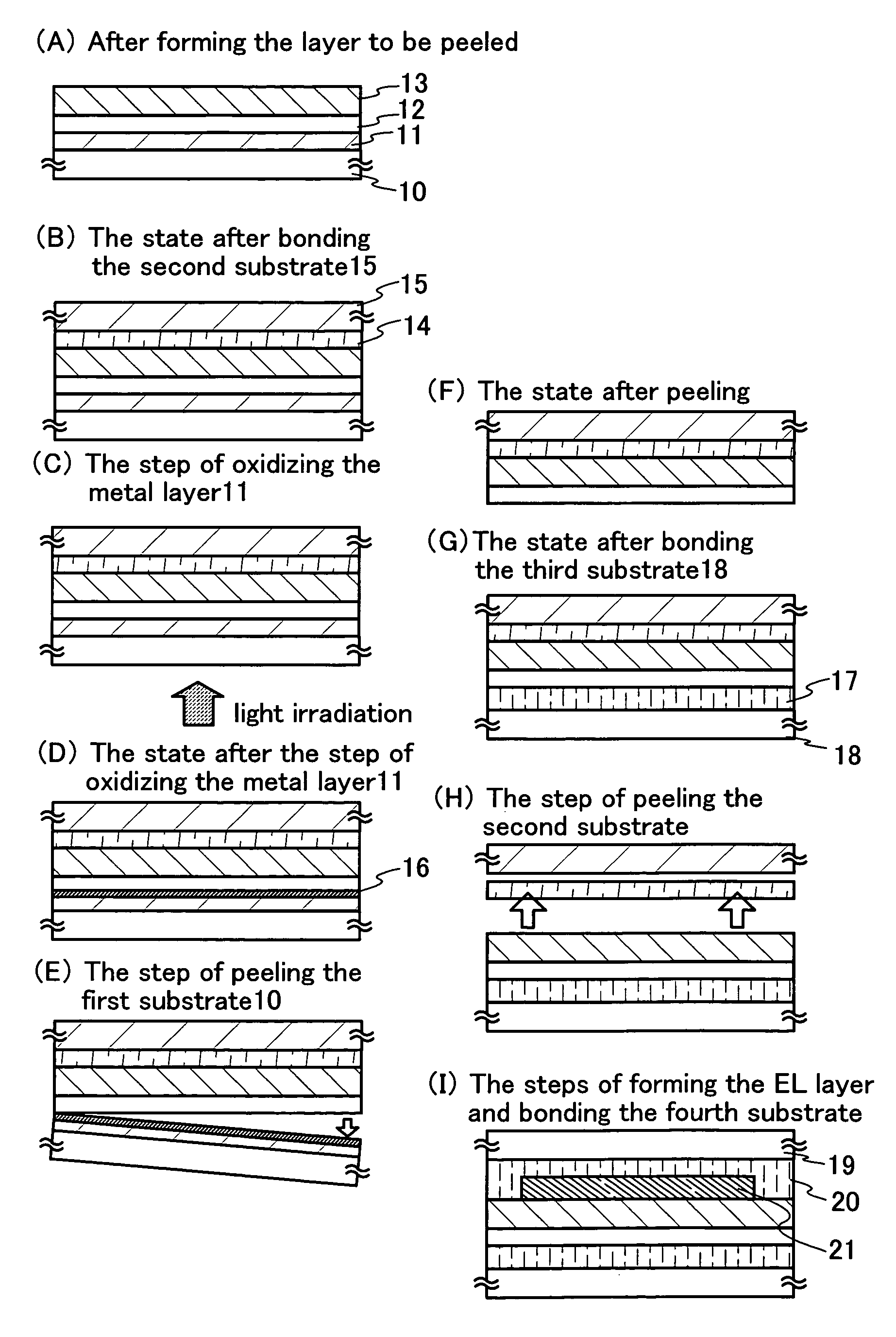
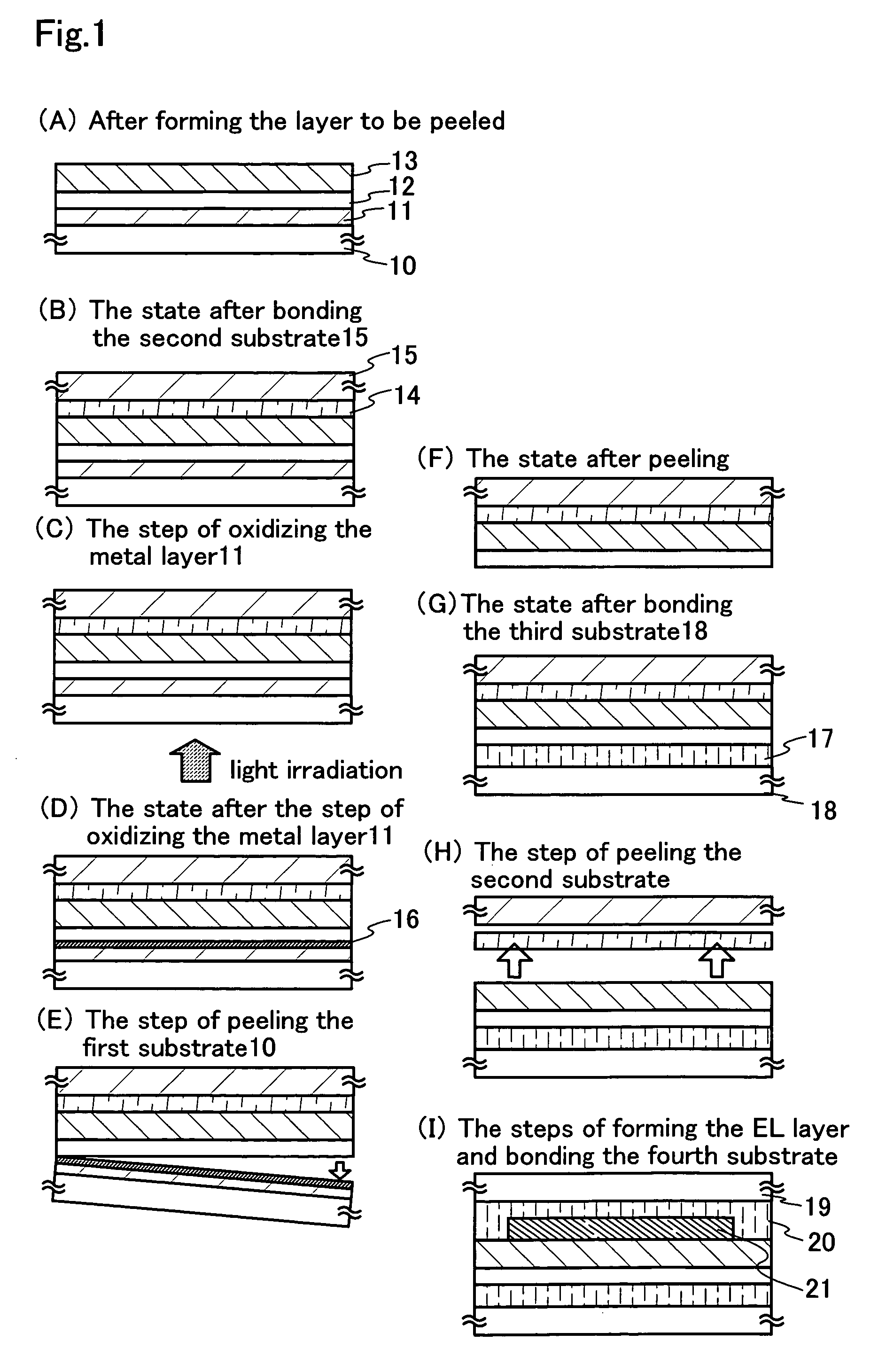
[0080]An embodiment of the present invention will be described with reference to FIGS. 3 to 7. Here, a method for manufacturing a pixel portion and TFTs (n-channel TFTs and a p-channel TFT) of a driver circuit provided at the periphery of the pixel portion at the same time on the same substrate will be described in detail. Although an example of manufacturing an active matrix substrate for manufacturing a reflective liquid crystal display device will be shown here, there is no limitation. When an arrangement of TFTs and a material of a pixel electrode are appropriately changed, needless to say, it is also possible to manufacture a transmissive liquid crystal display device and a light-emitting device that has a light-emitting layer including an organic compound.

[0081]A glass substrate (AN100) is used as a substrate 100. First, a silicon oxynitride layer 101 is formed on the substrate with PCVD to be a thickness of 100 nm.
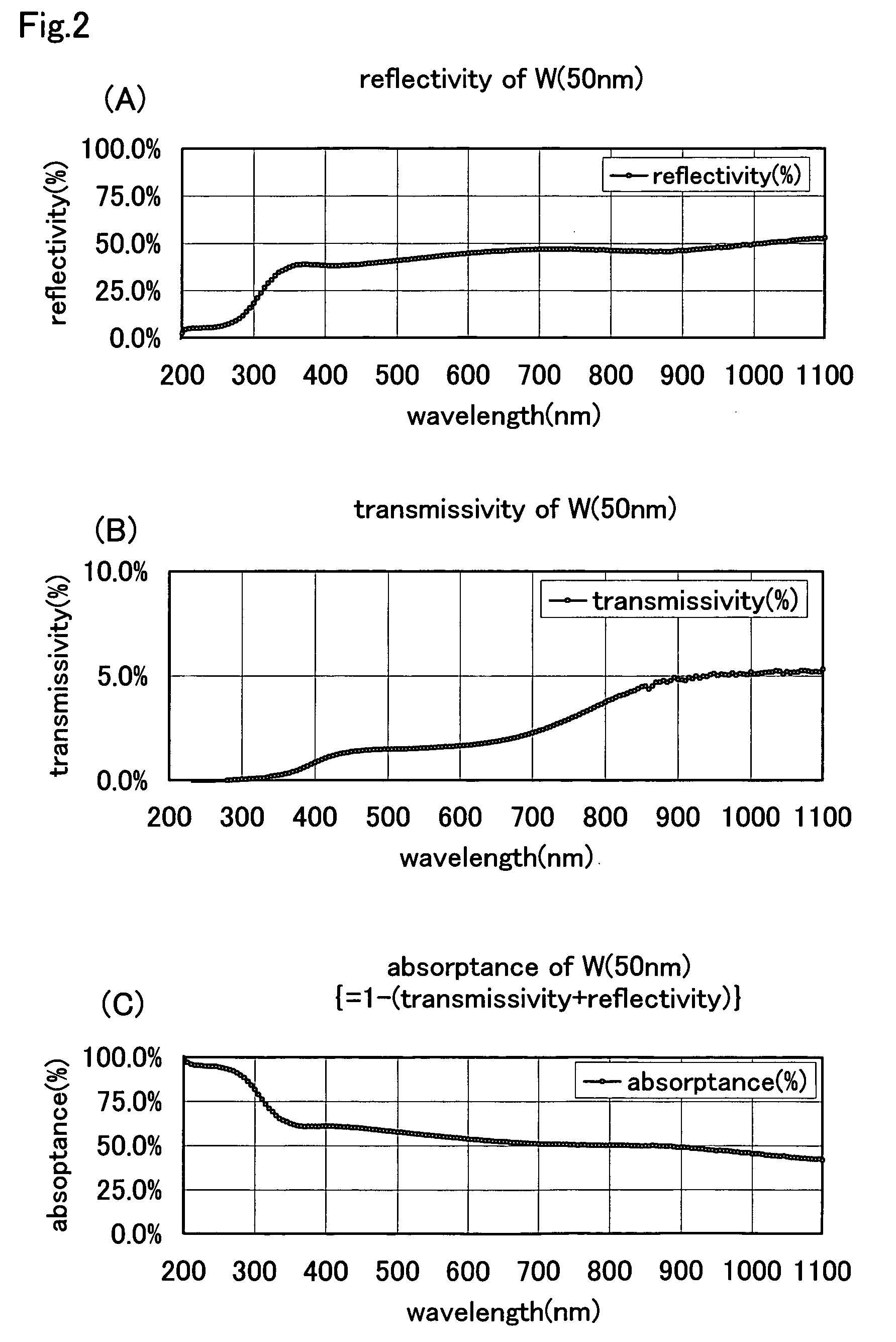
[0082]Subsequently, as a metal layer, a tungsten...

Example

[Embodiment 2]

[0134]Embodiment 1 shows an example of a reflective display device in which a pixel electrode is formed of a reflective metal material. In the present embodiment, an example of a transmissive display device, in which a pixel electrode is formed of a light-transmitting conductive film, is shown in FIG. 8.

[0135]Since processes up to the step of forming an interlayer insulating film are the same as those of Embodiment 1, the description thereof is omitted here. After forming the interlayer insulating film in accordance with Embodiment 1, a pixel electrode 601 of a light-transmitting conductive film is formed. As the conductive film with transmittance, ITO (indium tin oxide alloy), indium oxide-zinc oxide alloy (In2O3—ZnO), zinc oxide (ZnO) film, and the like may be used.

[0136]Thereafter, contact holes are formed in an interlayer insulating film 600. Then, a connecting electrode 602 overlapping with the pixel electrode is formed. This connecting electrode 602 is connected ...

Example

[Embodiment 3]

[0139]In the present embodiment, an example for manufacturing a light-emitting device equipped with a light-emitting element that has a light-emitting layer including an organic compound, which formed on a plastic substrate will be described with reference to FIG. 9.

[0140]FIG. 9(A) is a top view that shows a light-emitting device and FIG. 9(B) is a sectional view of FIG. 9(A) taken along A–A′. A dotted line 1101 denotes a source signal line driver circuit, reference numeral 1102 denotes a pixel portion, and reference numeral 1103 denotes a gate signal line driver circuit. Reference numeral 1104 denotes a sealing substrate and reference numeral 1105 is a sealing agent. The inside surrounded by the first sealing agent 1105 is filled with a second transparent sealing material 1107.

[0141]Reference numeral 1108 is a wiring for transmitting signals to be input to the source signal line driver circuit 1101 and the gate signal line driver circuit 1103, and receives a video sig...


PUM


Abstract

It is an object of the present invention to provide a peeling method that causes no damage to a layer to be peeled and to allow not only a layer to be peeled with a small surface area but also a layer to be peeled with a large surface area to be peeled entirely. Further, it is also an object of the present invention to bond a layer to be peeled to various base materials to provide a lighter semiconductor device and a manufacturing method thereof. Particularly, it is an object to bond various elements typified by a TFT, (a thin film diode, a photoelectric conversion element comprising a PIN junction of silicon, or a silicon resistance element) to a flexible film to provide a lighter semiconductor device and a manufacturing method thereof.
When a metal layer 11 is provided over a substrate, an oxide layer 12 is provided in contact with the metal layer 11, a layer to be peeled 13 is formed, and the metal layer 11 is irradiated with a laser beam to perform oxidization and form a metal oxide layer 16, a clear separation is possible with a physical means within the metal oxide layer 12 or at an interface between the metal oxide layer 16 and the oxide layer 12.

Description

TECHINICAL FIELD[0001]The present invention relates to a peeling method of a layer to be peeled, especially, a method for peeling a layer to be peeled including various elements. In addition, the present invention relates to a semiconductor device that has a semiconductor integrated circuit or a thin film transistor (hereinafter referred to as TFT) transferred by sticking a separated layer to be peeled to a substrate, and a manufacturing method thereof. The invention relates, for example, an electro-optical device typified by a liquid crystal module, a light-emitting device typified by an EL module, and an electronics that has such a device mounted as a component.[0002]In the specification, the term, ‘semiconductor device’, generally indicates devices that are capable of functioning by utilizing semiconductor characteristics, and an electro-optical device, a light-emitting device, a semiconductor circuit, and electronics are all included in the semiconductor device.BACKGROUND ART[00...

Claims


Application Information

Patent Timeline
IPC IPC(8): H01L21/30H01L21/84H01L21/336H01L21/77H01L27/12H01L29/786
CPCH01L27/1214H01L27/1266H01L29/78603H01L51/0024H01L51/003H01L23/291H01L29/66757H01L2221/68368H01L2924/0002Y10S438/928Y10S438/982H01L2924/00H01L27/1218H10K71/50H10K71/80H01L27/12H10K59/12H10K71/10H10K71/60
Inventor YAMAZAKI, SHUNPEITAKAYAMA, TORUMARUYAMA, JUNYAOHNO, YUMIKO
Owner SEMICON ENERGY LAB CO LTD
Why Eureka
Try Eureka