Method of manufacturing a semiconductor structure comprising clusters and/or nanocrystal of silicon and a semiconductor structure of this kind

a technology of nanocrystals and semiconductors, applied in vacuum evaporation coatings, lasers, coatings, etc., can solve the problems of only rationally expanding the method to the production of a few, unable to achieve relatively small nanocrystal density, and the need for ion implantation is a substantial complication. achieve the effect of high cluster density and large-scale economic

Inactive Publication Date: 2007-05-22
MAX PLANCK GESELLSCHAFT ZUR FOERDERUNG DER WISSENSCHAFTEN EV
View PDF7 Cites 13 Cited by
  • Summary
  • Abstract
  • Description
  • Claims
  • Application Information

AI Technical Summary

Benefits of technology

[0016]The object underlying the present invention is to provide a method for the manufacture of clusters and/or nanocrystals of silicon which enables a semiconductor structure having a high density of clusters and/or nanocrystals to be achieved with the clusters and/o

Problems solved by technology

Although ion implantation can be used to produce silicon nanocrystals it has the significant disadvantage that large area ion implantation with a high Si ion dose is not regularly used in silicon electronic production systems and thus the need to use ion implantation is a substantial

Method used


Image

  • Method of manufacturing a semiconductor structure comprising clusters and/or nanocrystal of silicon and a semiconductor structure of this kind
  • Method of manufacturing a semiconductor structure comprising clusters and/or nanocrystal of silicon and a semiconductor structure of this kind
  • Method of manufacturing a semiconductor structure comprising clusters and/or nanocrystal of silicon and a semiconductor structure of this kind

Examples


Embodiment Construction

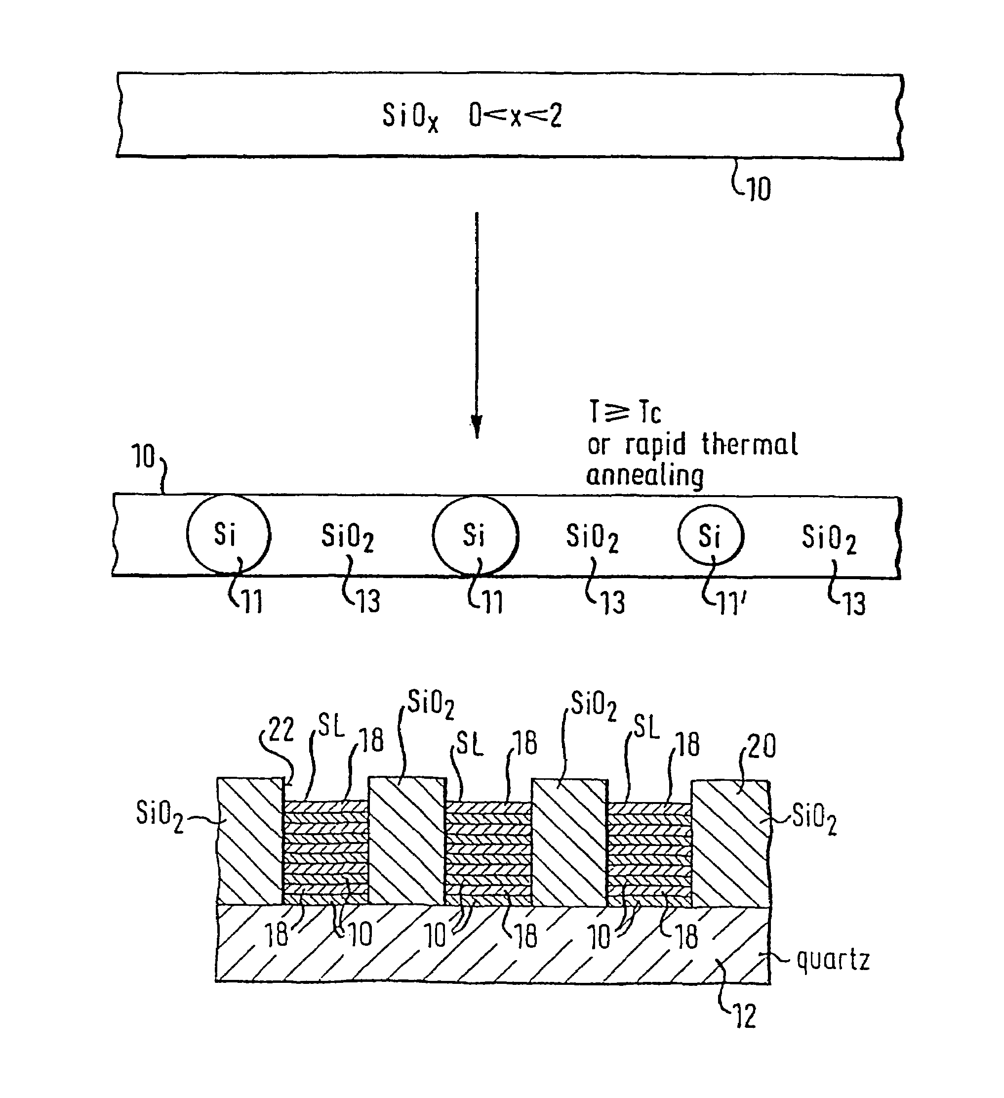
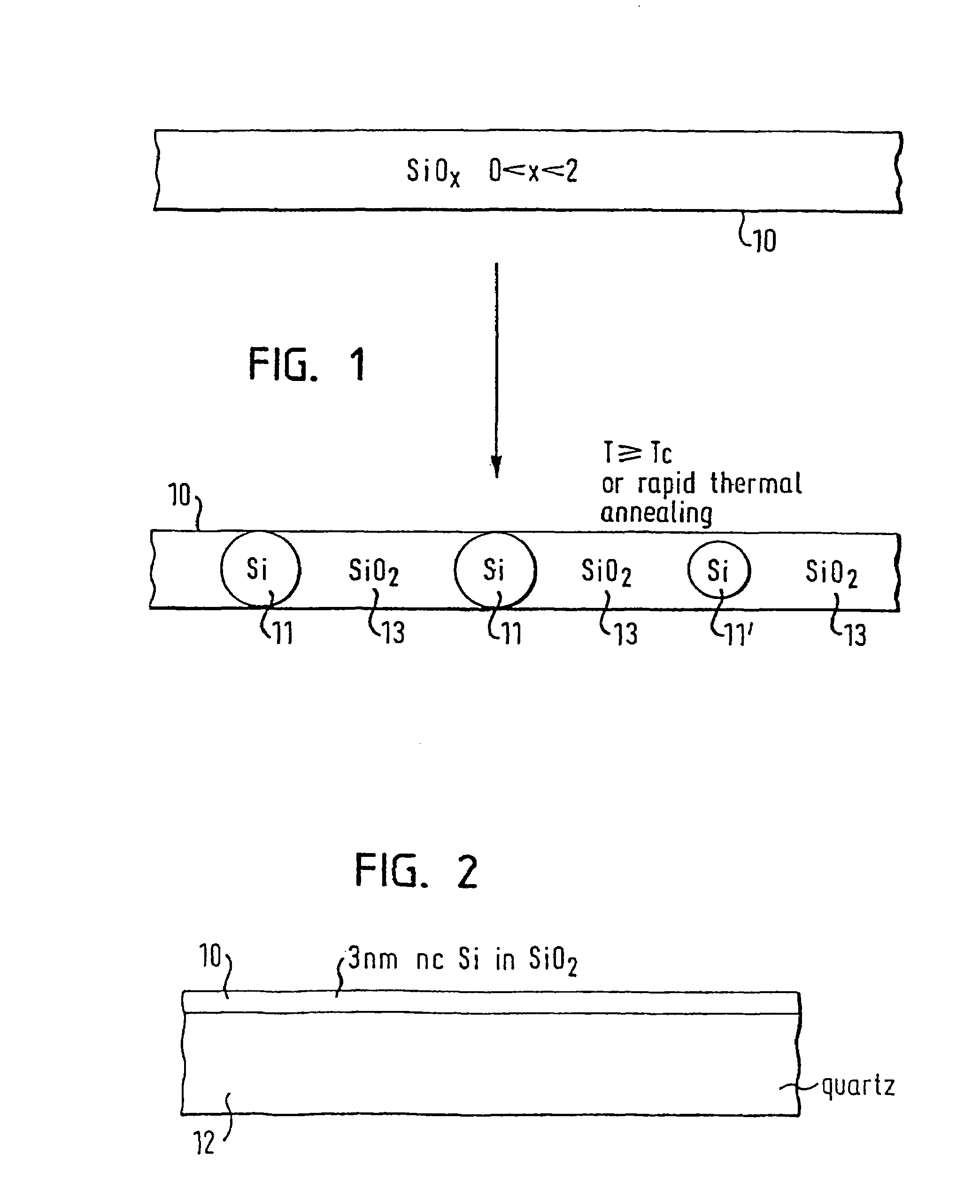
[0046]Turning now to FIG. 1 there is shown a schematic side view of a single layer 10 of a layer of a thermally non-stable silicon compound, here in the form of SiOx, with the value of x selected to be a non-stochiometric value greater than 0 but less than 2. The layer 10 can have a layer thickness in the range between 0.5 nm and 20 nm, but is preferably 2 to 3 nm thick. The layer 10 can be deposited by any of the known layer deposition processes such as a chemical vapor deposition, low-pressure chemical vapor deposition, evaporation of SiOx in oxygen containing atmospheres, sputtering, reactive sputtering, pulsed laser deposition and molecular beam epitaxy.

[0047]Although the thermally non-stable silicon compound used in all the present examples is SiOx, it is quite conceivable that other thermally non-stable silicon compounds can also be used, one possibility being a silicon nitride which would then be deposited in the form SiNx.

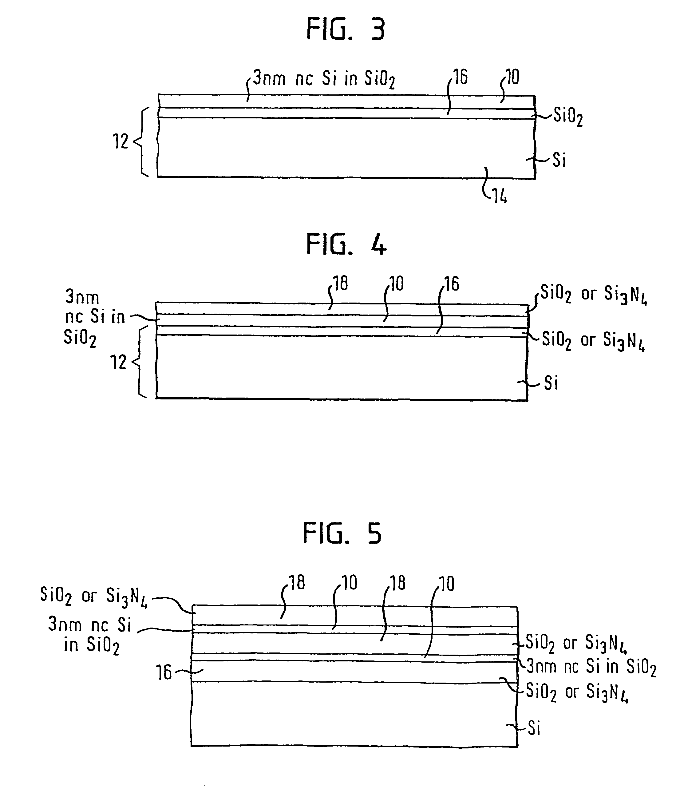
[0048]Having deposited the layer 10, it is then subje...


PUM

PropertyMeasurementUnit
Thicknessaaaaaaaaaa
Thicknessaaaaaaaaaa
Thicknessaaaaaaaaaa

Abstract

A method for manufacturing a semiconductor structure comprising clusters and/or nanocrystals of silicon described which are present in distributed form in a matrix of silicon compound. The method comprises the steps of depositing a layer of thermally nonstable silicon compound having a layer thickness in the range between 0.5 nm and 20 nm especially between 1 nm and 10 nm and in particular between 1 nm and 7 nm on a support and thermal treatment at a temperature sufficient to carry out a phase separation to obtain clusters or nanocrystals of silicon in a matrix of thermally stable silicon compound. The claims also cover semiconductor structures having such distributed clusters or nanocrystals of silicon The method described enables the economic production of high density arrays of silicon clusters or nanocrystals with a narrow size distribution.

Description

CROSS-REFERENCE TO RELATED APPLICATIONS[0001]This application claims filing date priority benefit to German application No. 101 04 193.4, filed Jan. 31, 2001, and to PCT application No. PCT / EP02 / 00860, filed Jan. 28, 2002, under 35 U.S.C. 119 which is explicitly incorporated by reference as if set forth below.BACKGROUND OF THE INVENTION[0002]1. Field of the Invention[0003]The present invention relates to a method of manufacturing a semiconductor structure comprising clusters and / or nanocrystals of silicon which are present in distributed form and a matrix of a silicon compound and to a semiconductor structure of this kind.[0004]2. Statement of the Prior Art[0005]It is known that Si clusters or nanocrystals embedded in SiO2 show a strong visible luminescence.[0006]There is currently much interest in designing semiconductor structures based on silicon which are able to emit light and which are suitable for integration into optoelectronic circuits in chip form, for example in the form ...

Claims


Application Information

Patent Timeline
IPC IPC(8): H01L21/00C23C14/06C23C16/30H01L33/08H01L33/34
CPCC23C14/06C23C16/30H01L33/08H01L33/34H01S3/169Y10S977/932Y10S977/814Y10S977/731
Inventor ZACHARIAS, MARGIT
Owner MAX PLANCK GESELLSCHAFT ZUR FOERDERUNG DER WISSENSCHAFTEN EV
Why Eureka
Try Eureka