Laser doping processing method and method for manufacturing semiconductor device

a technology of laser doping and processing method, which is applied in the direction of semiconductor devices, electrical devices, transistors, etc., can solve the problems of inability to accommodate wide-range doping, lack of reliability of threshold voltage, and large substrate size flowing through the fabrication process, so as to promote crystallization and promote crystallization. , excellent characteristics

Inactive Publication Date: 2009-03-17
SEMICON ENERGY LAB CO LTD
View PDF14 Cites 39 Cited by
  • Summary
  • Abstract
  • Description
  • Claims
  • Application Information

AI Technical Summary

Benefits of technology

[0020]In light of these problems, it is an object of the present invention to provide an easy doping method where concentration control is easy, where doping with respect to a large area can be practically conducted and which does not require a special device.
[0021]It is also an object of the invention to provide a doping method where concentration control in a depth direction that can accommodate shallow junctions can be easily conducted.
[0022]It is also an object of the invention to provide a gettering method that does not cause productivity and costs to deteriorate. Thus, the present invention provides a laser doping method where a liquid including a dopant (impurity of a conductivity type whose purpose is to control valence electrons) is applied to the surface of a semiconductor that is to be doped and the surface of the semiconductor is irradiated with laser light to add the dopant to the semiconductor.

Problems solved by technology

Although the threshold voltage is often used as a parameter to evaluate semiconductor devices, the threshold voltage lacks reliability if it is too high or too low, and the most important thing is being able to obtain a desired threshold voltage.
However, this is a problem because, when the gate length is shortened, the so-called short channel effect arises where the current leaks at the deep portion of the channel forming region.
The present state of affairs is one where there are problems with doping in that the sizes of substrates flowing through the fabrication process are becoming larger and the regions where doping is necessary are expanding in accompaniment with circuits that are becoming more integrated and displays that are becoming larger year after year.
For this reason, there are grave problems in that ion implantation cannot accommodate wide-range doping because doping cannot be conducted at one time over a wide range, and an enormous amount of time is required for processing in order to dope a large area.
With ion implantation, there is also the problem that it is necessary to implant ions with a low energy in order to form shallow junctions, but low-energy ion beams end up being emitted and it is difficult to obtain a sufficient current amount.
It is also extremely difficult to add the impurity to only the extremely shallow regions because the dopant ends up being diffused due to thermal annealing for recovering damage resulting from the ion implantation.
For this reason, there is a problem in applying plasma doping to channel doping, where precise concentration control is necessary.
With respect to laser doping, in methods that are often conducted where the semiconductor is irradiated with laser light in a dopant gas atmosphere, controlling the amount of the dopant to be implanted is difficult and a special device is required in order to uniformly distribute the dopant.
An other problem is that, although elements that promote crystallization have an extremely effective function in relation to crystallization, when these elements remain in large amounts in the semiconductor layer after crystallization, they have an adverse affect on TFT characteristics when a TFT—and particularly a TFT channel region—is made using the semiconductor layer.
In relation to removing the remaining element Ni, a method according to gettering (JP-A-10-214786) has been disclosed by the present applicant; however, a mask forming step for selectively adding the Ni element and a mask forming step for selectively adding a gettering element are necessary, and there is the problem of increasing steps, such as there being the necessity of having to twice conduct heating in the crystallization step and the gettering step, which causes productivity and costs to deteriorate.

Method used


Image

  • Laser doping processing method and method for manufacturing semiconductor device
  • Laser doping processing method and method for manufacturing semiconductor device
  • Laser doping processing method and method for manufacturing semiconductor device

Examples


embodiment 1

[0039]In the present embodiment, a method of doping a semiconductor by applying thereto a liquid including a dopant and irradiating the semiconductor with laser light will be described.

[0040]A liquid including a dopant is applied with a spinner to the surface of a semiconductor to form a thin film of the liquid including the dopant. An element that creates an N-type or a P-type is used as the dopant. Representative examples of the N-type include phosphor, arsenic and antimony, and representative examples of the P-type include boron, aluminium and gallium. The concentration of the dopant in the liquid is adjusted so that a desired concentration is eventually added to the semiconductor film.

[0041]Examples of the solution liquid including the element that creates the P-type or the N-type representatively include an aqueous solution of boric acid or phosphoric acid. When these aqueous solutions are applied to the surface of the semiconductor, the wettability between the semiconductor su...

embodiment 2

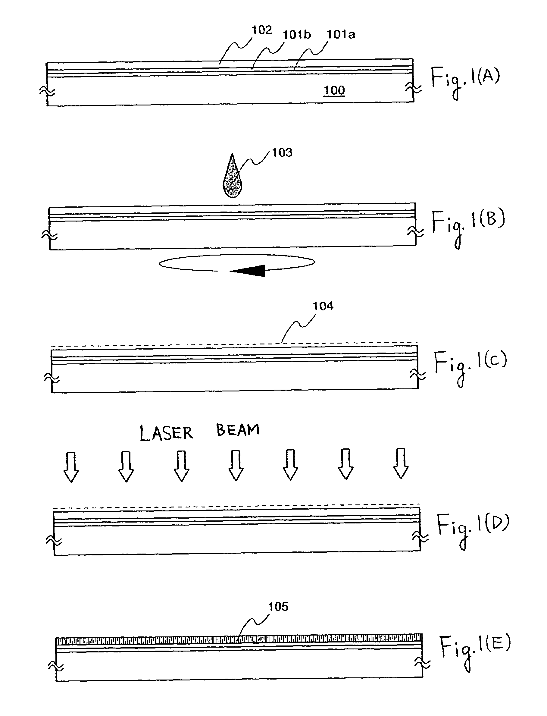
[0045]In the present embodiment, a method where crystallization and laser doping are simultaneously conducted will be described using FIG. 1.

[0046]First, base insulating films 101a and 101b are formed on a substrate 100. For the substrate, an insulating substrate such as a glass substrate, a quartz substrate, crystalline glass, or a ceramic substrate, a stainless steel substrate, a metal substrate (tantalum, tungsten, molybdenum, etc.), a semiconductor substrate, or a plastic substrate (polyimide, acrylic, polyethylene terephthalate, polycarbonate, polyarylate, polyethersulfone, etc.) can be used. A substrate that is suitable in consideration of the high temperature of the process and purpose may be selected from among these.

[0047]The base insulating films 101a and 101b are formed by forming a single layer or two or more plural layers of insulating films such as a silicon oxide film, a silicon nitride film or a silicon oxide nitride film. These are formed using a known method such a...

embodiment 3

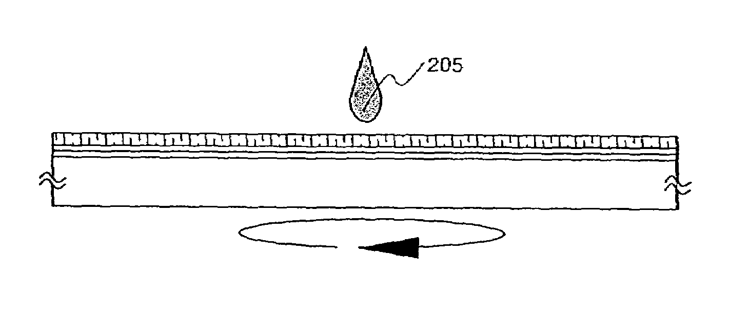
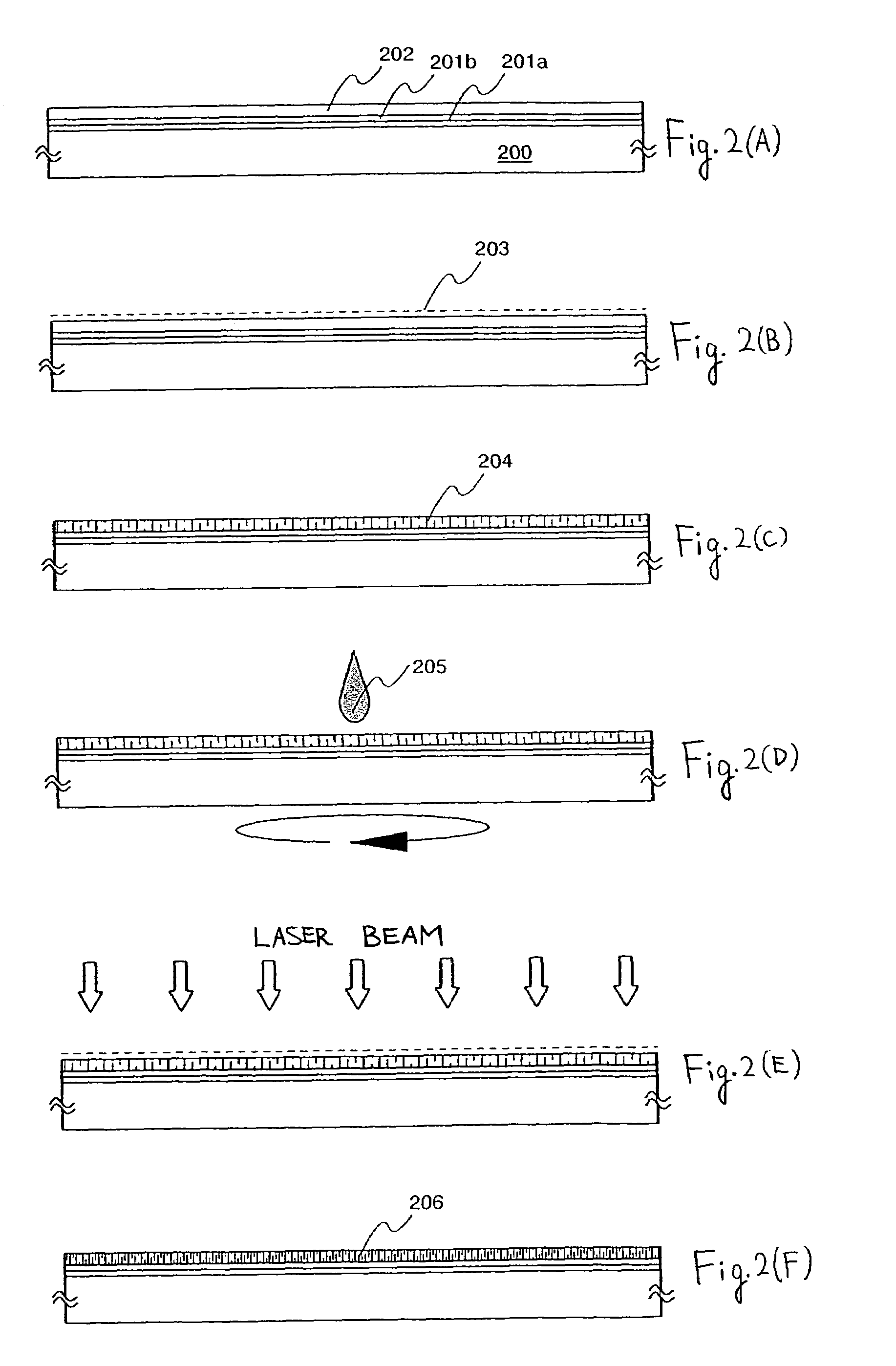
[0056]An other embodiment of the invention will be described using, FIG. 1 similar to Embodiment 2.

[0057]Similar to Embodiment 2, the base insulating films 101a and 101b are formed on the substrate 100, and the amorphous semiconductor layer 102 is formed thereon (FIG. 1(A)).

[0058]Next, an element that promotes crystallization is simultaneously incorporated, at a weight conversion of 5 to 100 ppm, in the liquid (boric acid aqueous solution) including the dopant (boron) and the liquid is applied to the amorphous semiconductor layer 102 with a spinner. In the present embodiment, nickel acetate corresponding to Ni at a weight conversion of 10 ppm is incorporated in the boric acid aqueous solution, and the thin film 104 of the liquid 103 including the dopant and Ni is formed on the amorphous semiconductor layer 102. Other examples of elements that promote crystallization include iron (Fe), palladium (Pd), tin (Sn), lead (Pb), cobalt (Co), platinum (Pt), copper (Cu) and gold (Au), but one...


PUM


Abstract

It is an object of the present invention to provide an easy doping method where concentration control is easy, where doping with respect to a large area can be practically conducted and which does not require a special device. The present invention provides a laser doping method where a liquid including a dopant is applied to the surface of a semiconductor that is to be doped and the surface of the semiconductor is irradiated with laser light to add the dopant to the semiconductor. It is also possible to conduct crystallization at the same time.

Description

BACKGROUND OF THE INVENTION[0001]1. Field of the Invention[0002]The present invention relates to a method of doping a semiconductor with an impurity. In particular, the present invention relates to channel doping, where precise control of the added amount of an impurity with which a semiconductor is to be doped is necessary, and to a laser doping method where an impurity is added to a semiconductor by irradiating the semiconductor with laser light.[0003]2. Description of the Related Art[0004]When a semiconductor device is fabricated using the electrical characteristics of a semiconductor, a technique called doping, where a minute amount of an impurity is added to a semiconductor in order to control the electrical characteristics thereof, is at present widely used. Methods of doping semiconductors can be broadly divided into two kinds: methods where the impurity is added in the process of forming the semiconductor from raw materials, and methods where the impurity is added after the ...

Claims


Application Information

Patent Timeline
Patent Type & Authority Patents(United States)
IPC IPC(8): H01L21/20H01L21/36H01L21/22H01L21/225H01L21/268H01L21/336H01L21/77H01L21/84H01L27/12H01L29/786
CPCH01L21/2255H01L21/268H01L27/12H01L29/66757H01L27/1277H01L21/0237H01L21/02532H01L21/02672H01L21/02675
Inventor KOEZUKA, JUNICHITAKADA, SADAKO
Owner SEMICON ENERGY LAB CO LTD
Why Eureka
Try Eureka