Photon counting imaging device

a technology of imaging device and photon, which is applied in the direction of x-ray photon detection device, x-ray/gamma/cosmic radiation measurement, instruments, etc., can solve the problems of inability to use high-dynamic investigation devices for x-ray photon detection, insufficient time resolution, and limited electronic circuitry, so as to facilitate observation even very fast changes and sufficient time resolution

Active Publication Date: 2009-04-07
DECTRIS LTD
View PDF13 Cites 38 Cited by
  • Summary
  • Abstract
  • Description
  • Claims
  • Application Information

AI Technical Summary

Benefits of technology

[0072]In order to achieve a sufficient time resolution the counting of the clock means should be initiated with the initial start of an experiment or a sample period. Therefore, it is useful when the external or the internal clock means can be reset and operates with a frequency in the range of 10 to 500 MHz, preferably about 100 MHz. The latter frequency yields to a time resolution of about 10 ns, which allows conveniently to observe even very fast changements in the crystalline structure of a probe.

Problems solved by technology

This change in potential causes the high-gain buffer amplifier to present a sufficiently large voltage change at the output of the amplifier to be above the system noise level.
The drawback of this disclosure remains substantially in the design of this photon counting device that is dedicated to detect with brilliant sensitivity a single photon having its energy in the range of the visible light (several eV).
This photon detecting device is therefore completely useless for the above-mentioned purposes of x-ray photon detection.
But even this device for x-ray photon detection can not be used in high dynamic investigation since the electronic circuitry is limited due to the switching dead time that is required to integrate the charge of the photo electrons subsequently to a chain of capacitors (referred to as a M-bit shift register) which have to be read out afterwards serially due to its chain-like arrangement.
It could be easily understood that the performance of this circuitry is limited to its switching intervals for charging and scanning the capacitors.
Unfortunately, the accumulated charge is stored as analog data using a circuitry having two transistors, one transistor acting as the charge store while the other acts as a readout switch responsive to an enable signal.
This circuitry does not enable any further manipulation of the pixel detector cells.
The main drawback of this arrangement consists in the susceptibility to a failure of a complete row of the detector array if only one the readout circuitry in a row fails.

Method used


Image

  • Photon counting imaging device
  • Photon counting imaging device
  • Photon counting imaging device

Examples


Embodiment Construction

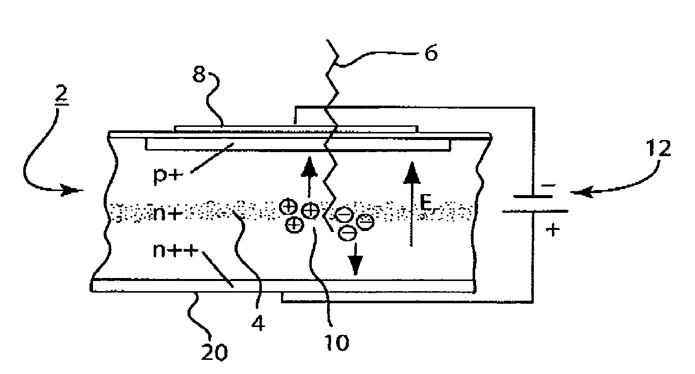
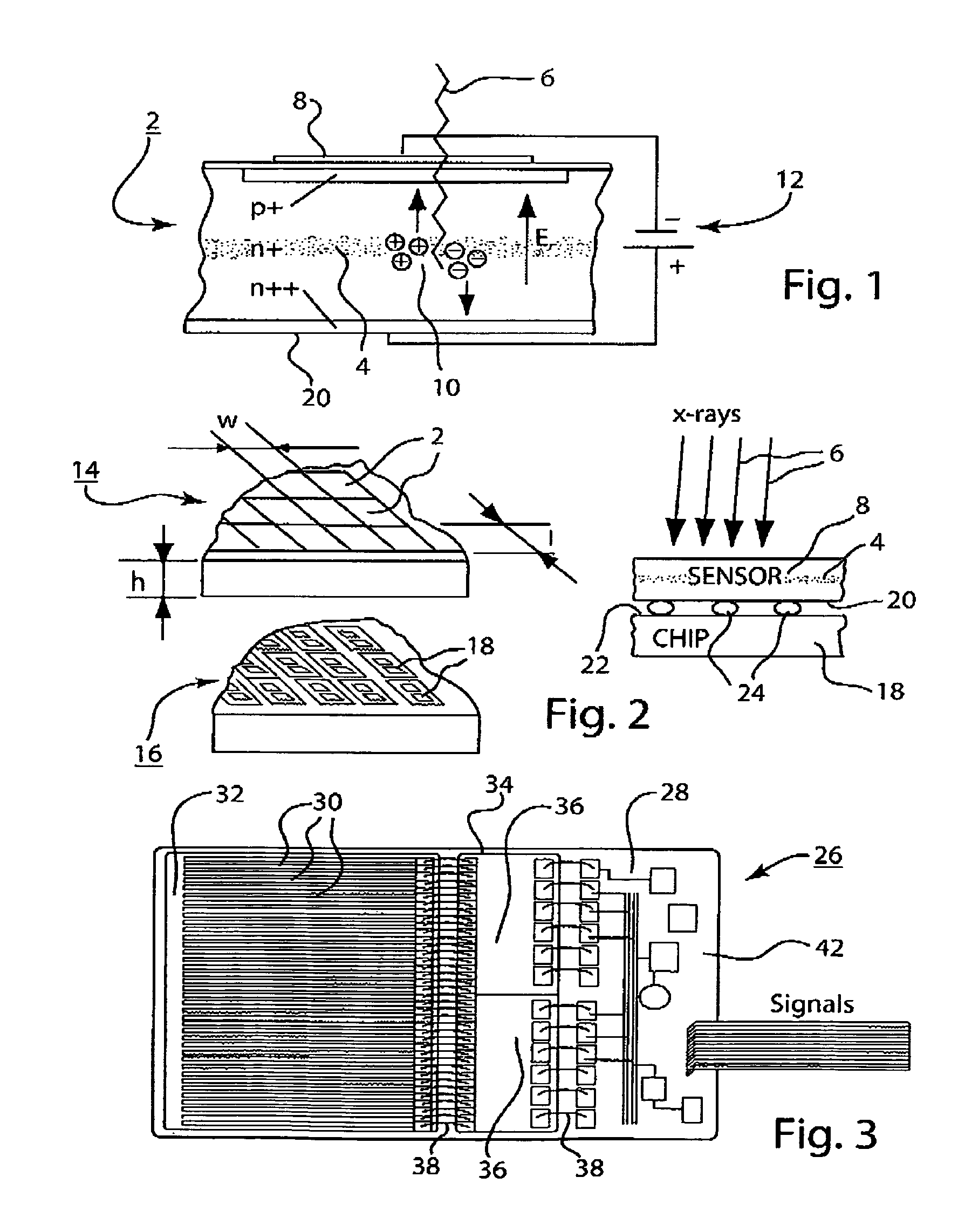
[0084]FIG. 1 illustrates schematically the architecture of a photodetector diode 2 having a doped semiconductor p+, n+, n++ trespassing section 4. The material chosen for the photodetector diode 2 depends on the desired bandgap energy required to generate an electron hole pair by the photo-effect. Suitable materials are undoped amorphous silicon having band gap of 1.12 eV and a bundle of IV-IV compounds and III-V compounds (indium and gallium salts, like gallium arsenide or indium antimonide).

[0085]An incident photon 6 having an energy in the range of several KeV before entering the doped semiconductor p+, n+, n++ trespassing section 4 passes through an aluminum cover layer 8 and causes according to its energy and to the energy gap of the doped semiconductor p+, n+, n++ trespassing section 4 a respective number of electron hole pairs 10 under x-ray annihilation. In the drawings, this number of electron hole pairs is exemplarily shown by one electron-hole pair 10 being divided by the...


PUM


Abstract

The invention is directed to increasing the time resolution capabilities of a photon counting imaging device. This is achieved by a photon-counting imaging device for single x-ray counting, including: a layer of photosensitive material; an N×M array of photodetector diodes arranged in the layer of the photosensitive material; an N×M array of readout unit cells including an high gain, low noise amplifying elements, one readout unit cell for each photodetector diode; the readout unit cells being controlled by a data processing elements; each readout unit cell comprising an internal data processing elements allowing to assign an output signal representing an amplifyied signal of the electron hole pairs generated by an incident photon or a predetermined number of incident photons in the respective photodetector diode to a preselectable region of interest; and the assignment of the output signal is accompanied by a time stamp generated by a clock means.

Description

BACKGROUND OF THE INVENTION[0001]The invention relates to a photon-counting imaging device for single x-ray counting. Further, the invention relates to a photon-counting imaging device with a fast region of interest data evaluation.[0002]X-ray diffraction patterns are useful in the analysis of molecular structures, such as protein and virus molecules, and require photon counting imaging devices. Especially, protein and virus crystallography imposes stringent requirements on x-ray detectors, particularly where the x-ray source is high flux synchrotron radiation that enables an experiment to be done rapidly. Furthermore, an important and developing field is time-resolved diffraction experiments using synchrotron radiation, such as crystallography and / or powder diffraction analysis. Monitoring a time-dependent reaction in a sample, i.e. a crystal or a powder, can elucidate the time-dependent crystal / molecular changes that occur in a chemical reaction as well. High time resolution speed...

Claims


Application Information

Patent Timeline
Patent Type & Authority Patents(United States)
IPC IPC(8): G01T1/20G01T1/00H01L27/146H01L31/115
CPCH01L27/14661
Inventor BROENNIMANN, CHRISTIANSCHMITT, BERND
Owner DECTRIS LTD
Why Eureka
Try Eureka