Manufacturing method of SOI substrate and manufacturing method of semiconductor device

a manufacturing method and semiconductor technology, applied in the direction of semiconductor devices, electrical equipment, basic electric elements, etc., can solve the problems of glass substrate having low heat resistance, process temperature limit in manufacturing transistors, and soi substrate after bonding a single-crystalline silicon layer cannot be heated at a temperature, etc., to achieve high surface planarity, low heat resistance, and high surface planarity

Inactive Publication Date: 2010-10-26
SEMICON ENERGY LAB CO LTD
View PDF51 Cites 17 Cited by
  • Summary
  • Abstract
  • Description
  • Claims
  • Application Information

AI Technical Summary

Benefits of technology

[0013]In other words, when a transistor is manufactured using an SOI substrate in which a silicon layer is bonded to a glass substrate by a conventional technique, it is difficult to sufficiently obtain characteristics which can be realized with an SOI substrate. In consideration of these problems, it is an object of the present invention to provide a manufacturing method of an SOI substrate with which a semiconductor device with high performance can be manufactured, even in the case of using a substrate having low heat resistance such as a glass substrate as a base substrate. Further, it is another object of the present invention to provide a manufacturing method of an SOI substrate which enables manufacturing of a semiconductor device with high performance, even in the case of introducing ions by an ion doping apparatus.
[0018]Then, the semiconductor layer is irradiated with laser light to be melted. This process improves planarity of a separation plane of the semiconductor layer and reduces crystal defects of the semiconductor layer. After laser light irradiation, the semiconductor layer is thinned. The thickness of the semiconductor layer is preferably equal to or less than 100 nm and more preferably equal to or less than 50 nm.
[0020]By thinning a semiconductor layer after laser light irradiation, an SOI substrate which includes a thin semiconductor layer with high surface planarity and in which a substrate having low heat resistance such as a glass substrate is used as a base substrate, can be manufactured. Even when an ion doping apparatus for which a mass separation function is not provided is used in forming an ion introduction layer, an SOI substrate including a thin semiconductor layer with high surface planarity can be manufactured. Accordingly, by using an SOI substrate of the present invention, a semiconductor device with high added value such as high integration, high speed driving, and low power consumption can be manufactured.

Problems solved by technology

However, the strain point of the glass substrate is equal to or lower than 700° C., and thus the glass substrate has low heat resistance.
Therefore, an SOI substrate after bonding a single-crystalline silicon layer cannot be heated at a temperature which exceeds a heat resistance temperature of the glass substrate, and the process temperature in manufacturing an SOI substrate is limited to be equal to or lower than 700° C.
In addition, there is also a process temperature limit in manufacturing a transistor using a single-crystalline silicon layer bonded to a glass substrate.
Further, since the substrate is large, the apparatus and the processing method which can be used are naturally limited.
However, it is difficult to remove the projections and depressions of the single-crystalline silicon layer which is bonded to a large-sized glass substrate by mechanical polishing with high throughput because the glass substrate and the silicon wafer have different shapes and sizes, and so on.
However, since the mass of a hydrogen element is small, it is difficult to introduce hydrogen ions at a depth equal to or less than 50 nm, and in addition, it is difficult to separate a silicon layer having a thickness of equal to or less than 50 nm from a silicon wafer.
In particular, in the case where hydrogen ions are introduced by an ion doping apparatus with which ions of a source gas are introduced without mass separation, it is very difficult to evenly introduce hydrogen ions to a depth of equal to or less than 100 nm.

Method used


Image

  • Manufacturing method of SOI substrate and manufacturing method of semiconductor device
  • Manufacturing method of SOI substrate and manufacturing method of semiconductor device
  • Manufacturing method of SOI substrate and manufacturing method of semiconductor device

Examples


embodiment mode 1

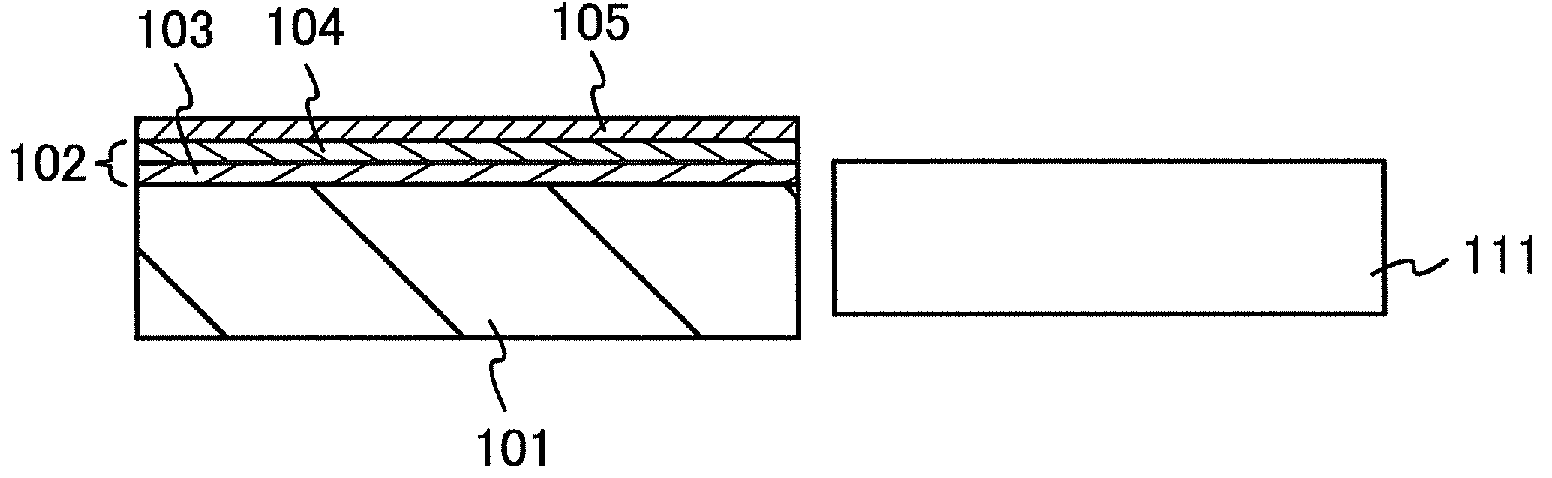
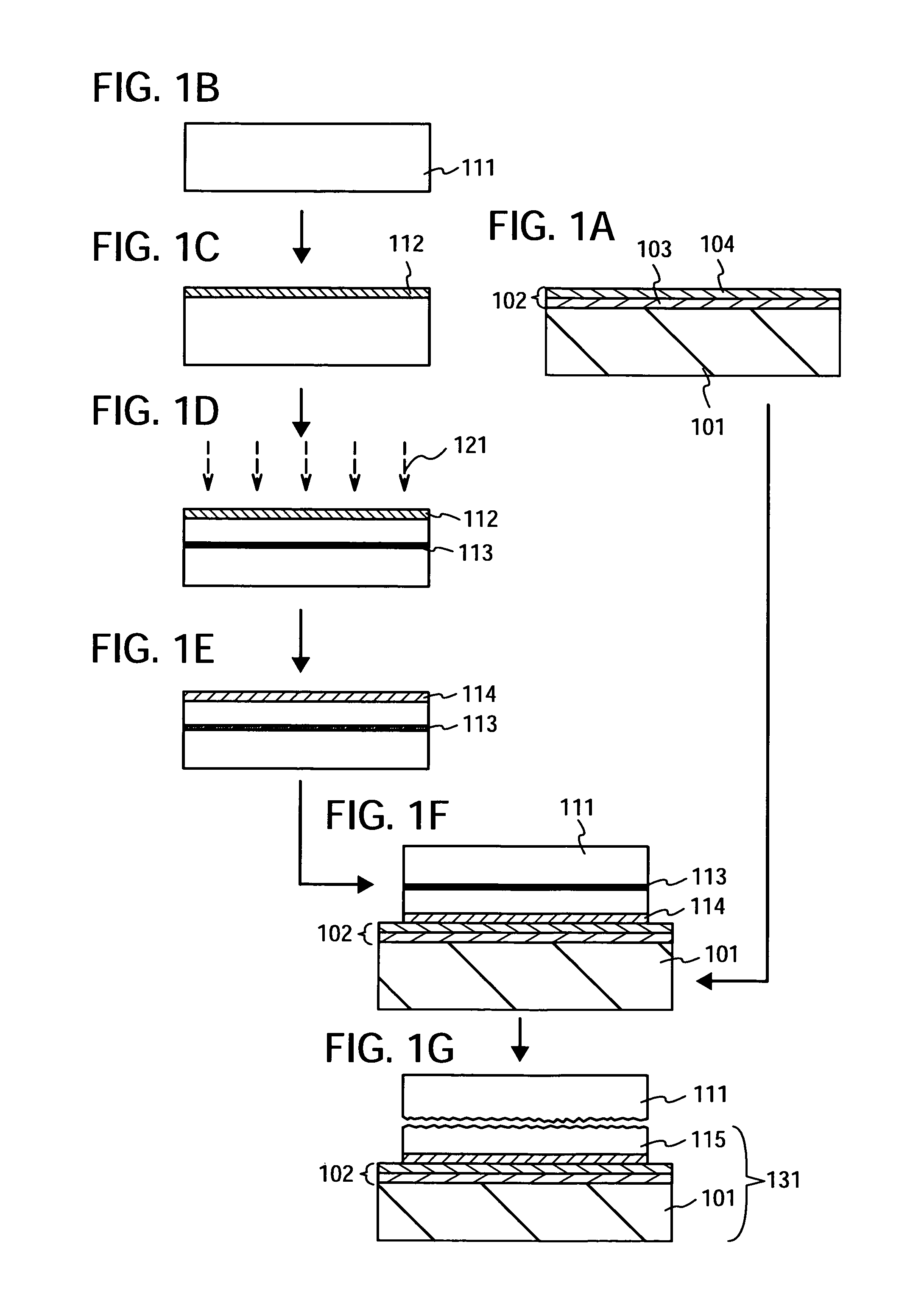
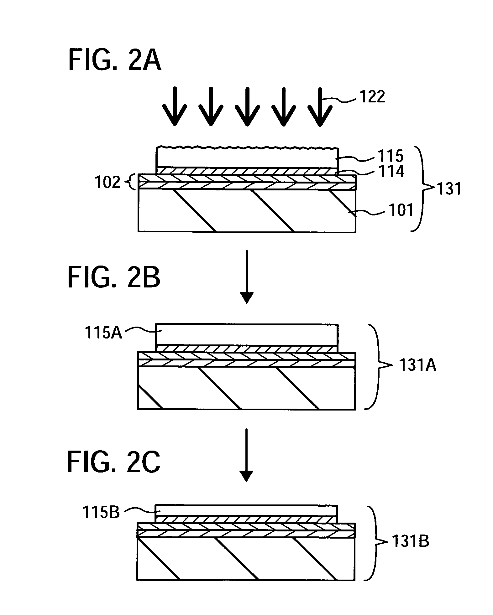
[0070]FIGS. 1A to 2C are cross-sectional views showing an example of a manufacturing method of an SOI substrate. With reference to FIGS. 1A to 2C, an example of a manufacturing method of an SOI substrate is described.

[0071]As shown in FIG. 1A, a base substrate of an SOI substrate 101 is prepared. As the base substrate 101, a light-transmitting glass substrate used for the products of electronics industry such as a liquid crystal display device can be used. It is preferable to use a glass substrate having a coefficient of thermal expansion of equal to or higher than 25×10−7 / ° C. and equal to or lower than 50×10−7 / ° C. (preferably, equal to or higher than 30×10−7 / ° C. and equal to or lower than 40×10−7 / ° C.) and a strain point equal to or higher than 580° C. and equal to or lower than 680° C. (preferably, equal to or higher than 600° C. and equal to or lower than 680° C.) in terms of heat resistance, cost, and the like. Further, a non-alkali glass substrate is preferable as the glass ...

embodiment mode 2

[0119]FIGS. 3A to 4C are cross-sectional views showing an example of a manufacturing method of an SOI substrate. Hereinafter, the example of the manufacturing method of an SOI substrate is described with reference to FIGS. 3A to 4C.

[0120]As the above description with FIG. 1A, the base substrate 101 to be a base substrate of an SOI substrate is prepared. FIG. 3A is a cross-sectional view of the base substrate 101. As described with FIG. 1B, the semiconductor substrate 111 is prepared. FIG. 3B is a cross-sectional view of the semiconductor substrate 111.

[0121]The semiconductor substrate 111 is washed to be clean. Then, as shown in FIG. 3C, an insulating layer 116 is formed on an upper surface of the semiconductor substrate 111. The insulating layer 116 has a single-layer structure or a multilayer structure of two or more layers. The thickness of the insulating layer 116 can be equal to or greater than 10 nm and equal to or less than 400 nm.

[0122]As a film which forms the insulating la...

embodiment mode 3

[0143]FIGS. 5A to 6C are cross-sectional views showing an example of a manufacturing method of an SOI substrate. With reference to FIGS. 5A to 6C, the example of the manufacturing method of an SOI substrate will be described.

[0144]As the description with FIG. 1A, the base substrate 101 to be a base substrate of an SOI substrate is prepared, and the insulating layer 102 is formed over the base substrate. In this embodiment also, the insulating layer 102 is a film with a two-layer structure including the silicon nitride oxide film 103 and the silicon oxynitride film 104. Next, as shown in FIG. 5A, the bonding layer 105 is formed over the insulating layer 102. This bonding layer 105 can be formed similarly to the bonding layer 114 formed over the semiconductor substrate 111.

[0145]Next, FIGS. 5B to 5D are cross-sectional views showing the same steps as FIGS. 1B to 1D. As described in Embodiment Mode 1, the protective film 112 is formed over the semiconductor substrate 111, and the ion i...


PUM

PropertyMeasurementUnit
thicknessaaaaaaaaaa
heat resistanceaaaaaaaaaa
heat resistance temperatureaaaaaaaaaa

Abstract

A manufacturing method of an SOI substrate which possesses a base substrate having low heat resistance and a very thin semiconductor layer having high planarity is demonstrated. The method includes: implanting hydrogen ions into a semiconductor substrate to form an ion implantation layer; bonding the semiconductor substrate and a base substrate such as a glass substrate, placing a bonding layer therebetween; heating the substrates bonded to each other to separate the semiconductor substrate from the base substrate, leaving a thin semiconductor layer over the base substrate; irradiating the surface of the thin semiconductor layer with laser light to improve the planarity and recover the crystallinity of the thin semiconductor layer; and thinning the thin semiconductor layer. This method allows the formation of an SOI substrate which has a single-crystalline semiconductor layer with a thickness of 100 nm or less over a base substrate.

Description

BACKGROUND OF THE INVENTION[0001]1. Field of the Invention[0002]The present invention relates to a manufacturing method of an SOI (silicon on insulator) substrate including a semiconductor layer formed of a semiconductor material such as silicon.[0003]Note that semiconductor devices in this specification refer to general devices which can function by utilization of semiconductor characteristics, and electro-optical devices, semiconductor circuits, and electronic appliances are all semiconductor devices.[0004]2. Description of the Related Art[0005]Instead of a bulk silicon wafer, integrated circuits using an SOI (silicon on insulator) substrate in which a thin single-crystalline silicon layer is formed on an insulating layer have been developed. By utilizing characteristics of the thin single-crystalline silicon layer, transistors formed in the integrated circuit can be electrically separated from each other completely. Further, since the fully depleted transistors can be formed, a s...

Claims


Application Information

Patent Timeline
Patent Type & Authority Patents(United States)
IPC IPC(8): H01L21/46
CPCH01L21/76254H01L27/1214H01L51/0027H01L27/1266H01L2224/03552H01L29/78654H01L27/12H01L27/1203H10K71/421
Inventor MIYAIRI, HIDEKAZUSHIMOMURA, AKIHISAMIZOI, TATSUYAHIGA, EIJINAGANO, YOJI
Owner SEMICON ENERGY LAB CO LTD
Why Eureka
Try Eureka