Ultrathin nanoscale membranes, methods of making, and uses thereof

a technology of ultrathin nanoscale membranes and nano-scale particles, which is applied in the direction of basic electric elements, electrical equipment, water/sewage treatment, etc., can solve the problems of limiting process design flexibility and no simple alternatives, and achieves the effects of reducing processing requirements, high aspect ratio, and easy patterning and removal

Active Publication Date: 2011-04-12
UNIVERSITY OF ROCHESTER
View PDF83 Cites 30 Cited by
  • Summary
  • Abstract
  • Description
  • Claims
  • Application Information

AI Technical Summary

Benefits of technology

[0015]The single-side etching procedure described herein uses a different etching chemistry that allows a membrane formed of any material(s) to be locally released from the substrate with a single etching step, forming square edge-bound membranes. This greatly simplifies processing requirements because (i) for SiO2 films, this material is generally more accessible and easier to pattern and remove than SiN; (ii) KOH (a restricted contamination source in most clean rooms) is eliminated; and large area (500×500 μm2) ultrathin (<100 nm) membranes are formed with a single etching step requiring no additional thinning. The modified single-side etching procedure that utilizes sacrificial films to protect the ultrathin nanoscale membrane offers further advantages in being able to prepare membranes having a thickness of less than about 10 nm, and having high aspect ratios. Importantly, the procedures of the present invention avoid the need for mechanical polishing steps or ion beam etching procedures, which can cause damage to planar films in some circumstances and most certainly will cause damage to membranes that bear non-planar relief patterns.

Problems solved by technology

Although SiN is an excellent material choice for many applications, having no simple alternatives limits process design flexibility.

Method used


Image

  • Ultrathin nanoscale membranes, methods of making, and uses thereof
  • Ultrathin nanoscale membranes, methods of making, and uses thereof
  • Ultrathin nanoscale membranes, methods of making, and uses thereof

Examples


example 1

Formation of Silicon Dioxide Membranes

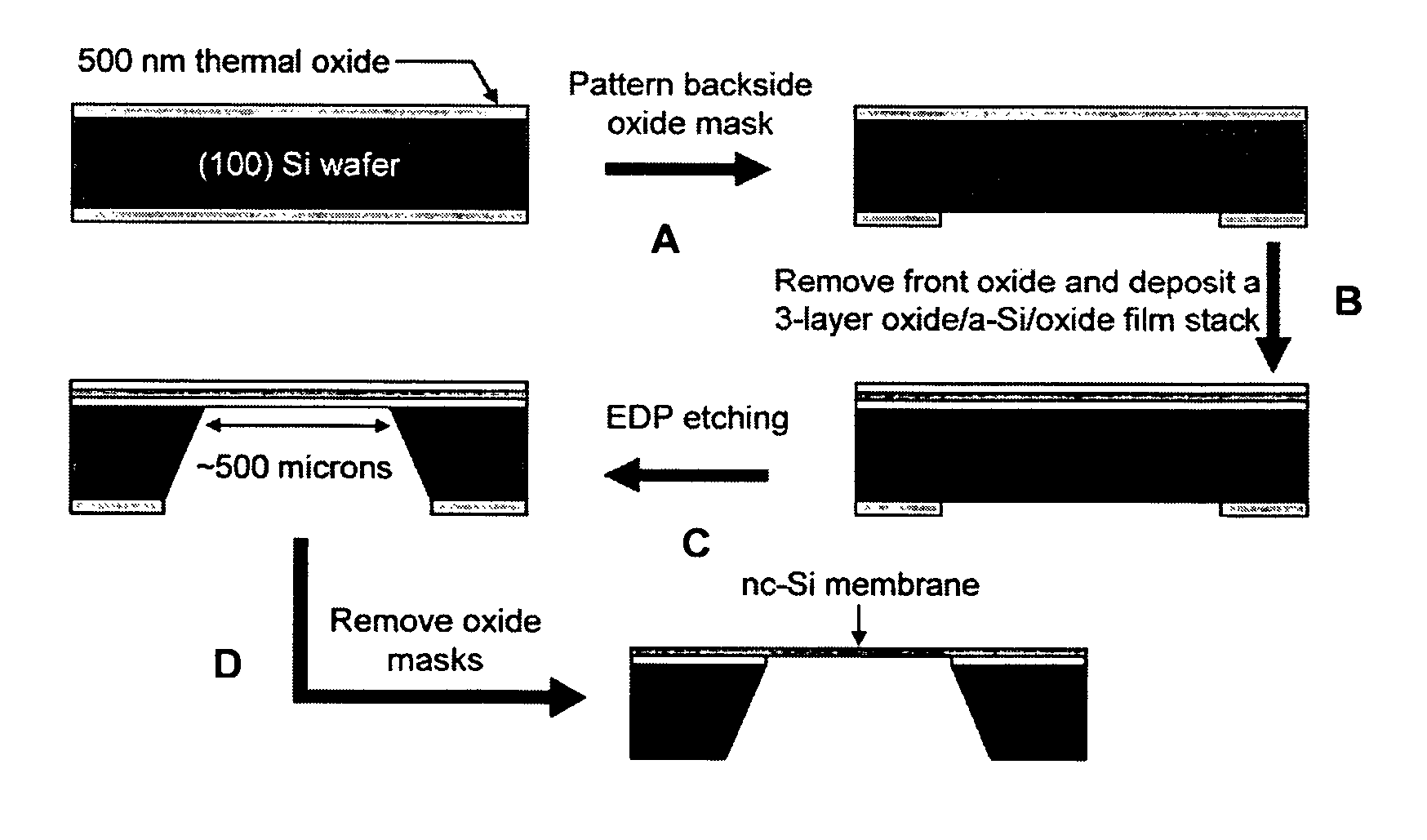
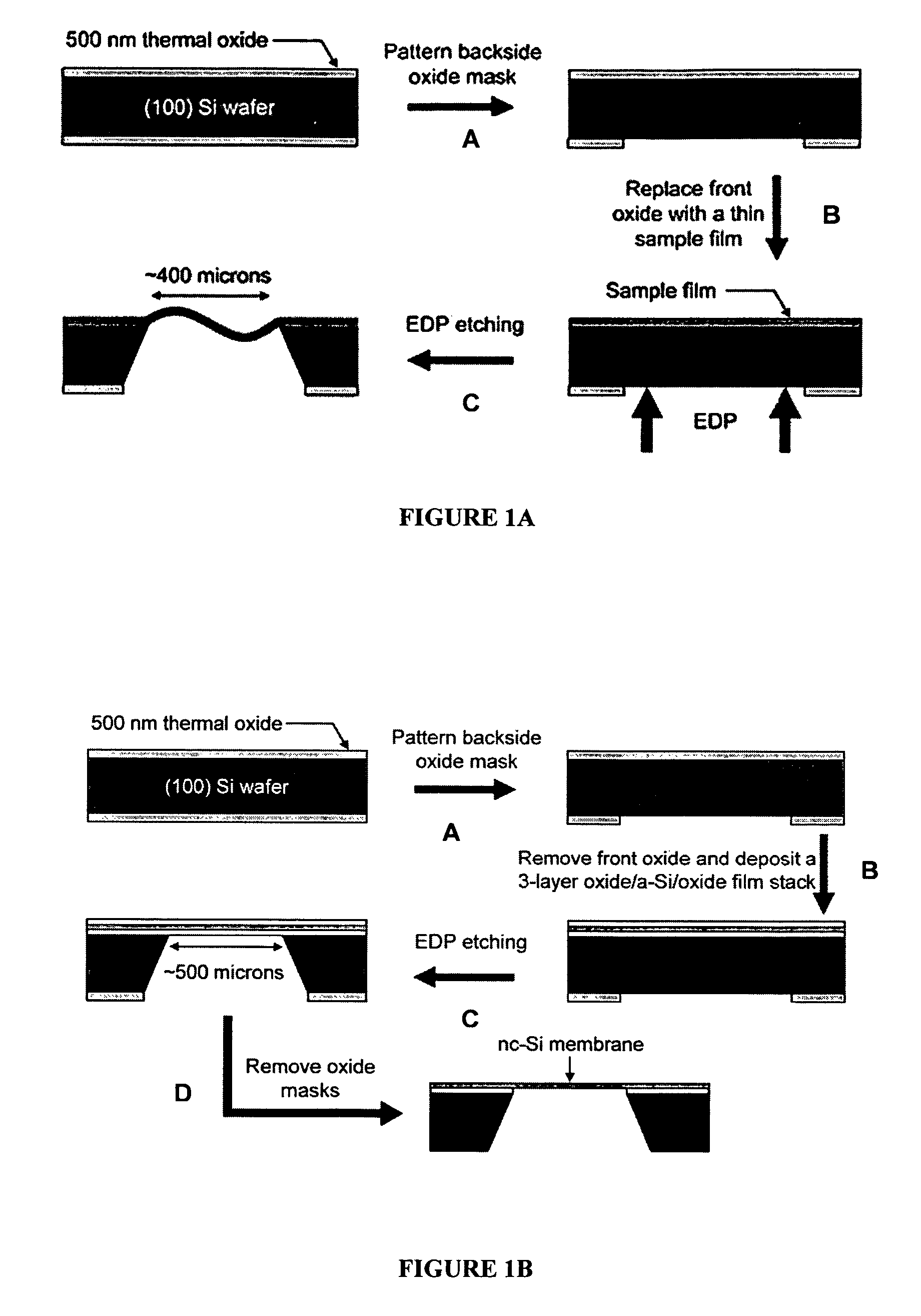
[0074]After having identified EDP as an anisotropic etchant capable of etching through the bulk of a silicon wafer and stopping abruptly on a thin oxide film, a process had to be engineered for this chemistry. An outline of such a procedure is shown in FIG. 1. This figure illustrates a through-wafer backside etching process graphically. Because SiO2 is so resistant to EDP, a 500 nm thermal oxide is adequate to mask the backside of the wafer (approx 500 microns thick) during the entire duration of the etch. This is quite advantageous since oxide is far easier to deposit, pattern, and remove than SiN, the standard masking layer for through wafer etches with KOH. As indicated in FIG. 1, after the growth of the mask oxide, the backside is patterned. During this patterning process, the front oxide protects the surface from damage induced by handling. The frontside oxide is then removed, and the sample layer of interest is deposited on the front surfa...

example 2

Formation of Nanocirystailine Silicon Membranes

[0078]Nc-Si membranes were fabricated by the procedure outlined in FIG. 1B. A 500 nm thick layer of SiO2 on both sides of a silicon wafer was first grown by placing it in a semiconductor tube furnace at 1000° C. for 2 hours in an ambient of oxygen and steam. On the backside of the wafer, the SiO2 is patterned using standard photolithography techniques to form an etch mask for the membrane formation process. The etch mask for each membrane included a square-shaped opening centrally positioned within a square border (up to 120 masks have been formed on a single silicon wafer). The front oxide layer was then removed by exposing the surface to 4:1 buffered oxide etchant, for 10 minutes in an etching cell similar to that used for EDP etching, and a high quality three layer film stack (20 nm-SiO2 / 15 nm-amorphous silicon / 20 nm-SiO2) was RF magnetron sputter deposited on the front surface. The a-Si layer was sputtered at a chamber pressure of 1...

example 3

Formation of Additional Nanocrystalline Silicon Membrane

[0083]The procedure described in Example 2 was used to form a 7 nm a-Si layer sandwiched between two 20 nm layers of SiO2 using sputter deposition (see FIG. 7B); the silicon was then annealed at 950° C. for 30 sec to form a nc-Si layer. After release, a wrinkled membrane similar to other oxide membranes was formed (FIG. 7A). However, after the removal of the sacrificial SiO2, with a 25 second dip in buffered oxide etch (BOE), an extremely flat 7 nm ne-Si membrane was produced (see FIGS. 7B-C). This dramatic shift from compressive to tensile stress was unexpected, yet is indicative of the volume contraction that occurs when a-Si is crystallized (Miura et al., Appl. Phys. Lett. 60:2746 (1992), Zacharias et al., Journal of Non-Crystalline Solids 227-230:1132 (1998), which are hereby incorporated by reference in their entirety). Since the oxide remains compressively stressed after annealing and is much thicker than the a-Si, the ov...


PUM

PropertyMeasurementUnit
surface roughnessaaaaaaaaaa
thicknessaaaaaaaaaa
thickaaaaaaaaaa

Abstract

A nanoscale membrane exposed on opposite sides thereof and having an average thickness of less than about 100 nm, and a lateral length to thickness aspect ratio that is more than 10,000 to 1 is disclosed. Also disclosed are methods of making such membranes, and use thereof in a number of devices including fuel cells, sensor devices, electrospray devices, and supports for examining a sample under electron microscopy.

Description

[0001]This application claims the benefit of U.S. Provisional Patent Application Ser. No. 60 / 676,375 filed Apr. 29, 2005, which is hereby incorporated by reference in its entirety.FIELD OF THE INVENTION[0002]The present invention is directed to ultrathin nanoscale membranes, methods of making the membranes, and uses thereof.BACKGROUND OF THE INVENTION[0003]Nearly all reported ultrathin microfabricated membranes are made of silicon nitride (SiN) (Deshmukh et al., “Nanofabrication Using a Stencil Mask,”Appl Phys Lett 75:1631-1633 (1999); and Toh et al., “Fabrication of Free-Standing Nanoscale Alumina Membranes with Controllable Pore Aspect Ratios,”Nano Lett 4:767-770 (2004)). This is because it is well known that the most commonly available anisotropic silicon etchant, potassium hydroxide (KOH), will not attack SiN. Therefore, a very large thickness of silicon (substrate) can be etched away while leaving a very small thickness of SiN, enabling the formation of thin membranes. Although...

Claims


Application Information

Patent Timeline
Patent Type & Authority Patents(United States)
IPC IPC(8): B01D53/22
CPCB01D67/0062B01D67/0072B01D69/02B01D71/02B01D71/022B01D71/024G03F7/0015H01M4/94B01D71/027B01D2325/08H01J2237/20H01M2250/00Y02E60/50B01D71/0221B01D71/0213B01D71/02231B01D71/0215
Inventor STRIEMER, CHRISTOPHER C.FAUCHET, PHILIPPE M.
Owner UNIVERSITY OF ROCHESTER
Why Eureka
Try Eureka