Displaying device and lighting device employing organic electroluminescence element

a technology of electroluminescence element and lighting device, which is applied in the direction of organic semiconductor devices, discharge tubes luminescnet screens, instruments, etc., can solve the problems of affecting the future exhaustion of light, difficult to adopt an ito electrode in the top emission type, and difficult to achieve the effect of el lighting device emitted light evenly from the whole surface, etc., and achieves the effect of effectively inhibiting and not particularly restricting the opening shap

Inactive Publication Date: 2011-04-19
KK TOSHIBA
View PDF9 Cites 12 Cited by
  • Summary
  • Abstract
  • Description
  • Claims
  • Application Information

AI Technical Summary

Benefits of technology

[0099]The present invention is aimed to reduce scattering effects and thereby to improve the efficiency of straightforwardness of light, and hence it is necessary to treat sizes perturbing the incident light as parameters when the surface structure is defined. From this viewpoint, it is found that the diameter of the opening is most properly determined by the radius of gyration of the opening structure and thereby that the efficiency of straightforwardness of light can be most properly represented. That is to say, the radius of the opening in the surface structure according to the present invention is defined as its radius of gyration, and accordingly the diameter is double the radius of gyration. Even if the openings have different shapes, the same effect of the invention can be obtained as long as the radii of gyration are the same. The radius of gyration is described in, for example, Iwanami Rikagaku Jiten (Iwanami's Dictionary of Physics and Chemistry, written in Japanese) 5th edition.
[0100]In the present invention, the radius of gyration of the opening is defined as follows. On an image of the opening, circular lines at equal intervals are drawn from the edge. In concrete, on a relief image obtained by atomic force microscopy, circular lines at equal intervals are drawn from the edge. The thus-obtained lines are image-processed to obtain the center of gravity. The distance from the center of gravity to the concavity is then determined, and is processed together with the moment to calculate the radius of gyration R. The radius of gyration can be also obtained by Fourier transform of the electron or atomic force micrograph.
[0101]The larger the surface structure is, the more light is scattered. The effect of light-scattering is in proportion to the square of the size. Accordingly, the average radius of gyration R of the openings is preferably not more than ⅙ of the wavelength of incident light. That is to say, the average diameter of the openings is preferably not more than ⅓ of the wavelength of incident light. As long as the above conditions are satisfied, the shapes of the openings are not particularly restricted. Examples of the opening shapes include cylindrical shape, conical shape, triangular pyramidal shape, quadrilateral pyramidal shape, and other columnar or pyramidal shapes. Two or more shapes may be mixed. Even if the light-transmitting metal electrode according to the present invention contains various sizes of openings, the effect of the invention can be obtained. It is, on the contrary, rather preferred that the openings have various sizes because the metal part with those openings is apt to continue linearly in a relatively long straight distance. In the case like the above, where the openings have various sizes, the diameters of the openings can be represented by the average.
[0102]Diffraction of light incident on the light-transmitting metal electrode used in the present invention is then described below. When light penetrates from the organic EL layer-side to the metal electrode-side, the scalar theory tells us as follows. The condition for causing diffraction is expressed by the following formula (2):nm×sin θm−ni×sin θi=m×λ / d  (2)in which θm is an emission angle from the metal electrode, θi is an incident angle from the organic EL layer-side, λ is a wavelength of incident light, d is an interval of diffraction grating, m is a diffraction order of integer (m=0, ±1, ±2, . . . ), and ni and nm are refractive indexes of the organic EL layer and a medium out of the metal electrode such as the transparent substrate, respectively. Accordingly, the condition for not causing diffraction is that the formula (2) does not have a solution when the diffraction order is the minimum: m=−1. This means that the condition is λ / ni<1, and hence the ratio of the wavelength of incident light per the refractive index of the transparent substrate is the threshold. The refractive index of organic EL layer generally used is not more than 2.0, and therefore the diffraction can be avoided if the intervals among the openings are not more than ½ of the wavelength of incident light. The openings are, therefore, preferably thus arranged.
[0103]The above openings are included in plural microdomains neighboring each other. The openings placed in each microdomain are arranged periodically, but the microdomains are so placed that the arranging direction of the openings in each microdomain is oriented at random. Otherwise, the openings are preferably arranged completely at random. According to the first theoretical basis, the reason for this can be explained as follows. For example, if the openings are arranged long-periodically in hexagonal symmetry, the metal part has areas periodically continued in tri-axial directions and therefore cannot inhibit the movement of free electrons isotropically. In the present invention, since the openings are arranged in a microdomain structure or in a random structure, the movement of free electrons can be effectively inhibited.
[0104]For analyzing and confirming relative positions of the openings, the following method can be adopted. For example, an electron or atomic force micrograph of the metal layer having the openings is subjected to two-dimensional Fourier transform to obtain, what is called, a “reciprocal lattice space image”. If the relative arrangement of the openings has periodicity, there are clear spots in the reciprocal lattice space image. In contrast, if the openings are relatively positioned isotropically, a ring is observed.

Problems solved by technology

Accordingly, it is difficult to adopt an ITO electrode in the top emission type organic EL display because a sputtering process or a high-temperature treatment is necessary to form the ITO electrode.
However, if a commonly used ITO layer is used as the light-transmitting electrode, it is difficult for the EL lighting device to emit light evenly from the whole surface.
Further, indium, which is a material of the ITO layer, is such a rare metal that exhaustion thereof in the future is now brought into a serious problem.
Accordingly, there is a fear that it will be difficult to procure indium in the future.
However, the semi-transparent metal electrode considerably lowers light-transparency to impair brightness of the resultant EL display seriously.
However, if the voltage is increased, heat is unfavorably generated to significantly shorten the working life-time of the display.
Further, it is difficult to evenly produce the very thin semi-transparent metal electrode if the display has a large displaying surface.
This means that a process margin in the procedures of forming the upper electrode becomes so small that the yield in mass-production is lowered.
Also in producing an organic EL lighting device, it is difficult to evenly produce the very thin semi-transparent metal electrode if the device has a large light-emitting surface.
In addition, if the electrode has a thickness enough to ensure high electrical conductivity, the light-transparency is impaired.
As described above, it has been difficult for the conventional light-transmitting electrode such as an ITO layer or a thin metal layer to be on a high level of both light-transparency and electrical conductivity.
However, even in this technology, the metal mesh electrode serves as only an assistant to the ITO layer and hence does not essentially solve the above problems.

Method used


Image

  • Displaying device and lighting device employing organic electroluminescence element
  • Displaying device and lighting device employing organic electroluminescence element
  • Displaying device and lighting device employing organic electroluminescence element

Examples


example 1

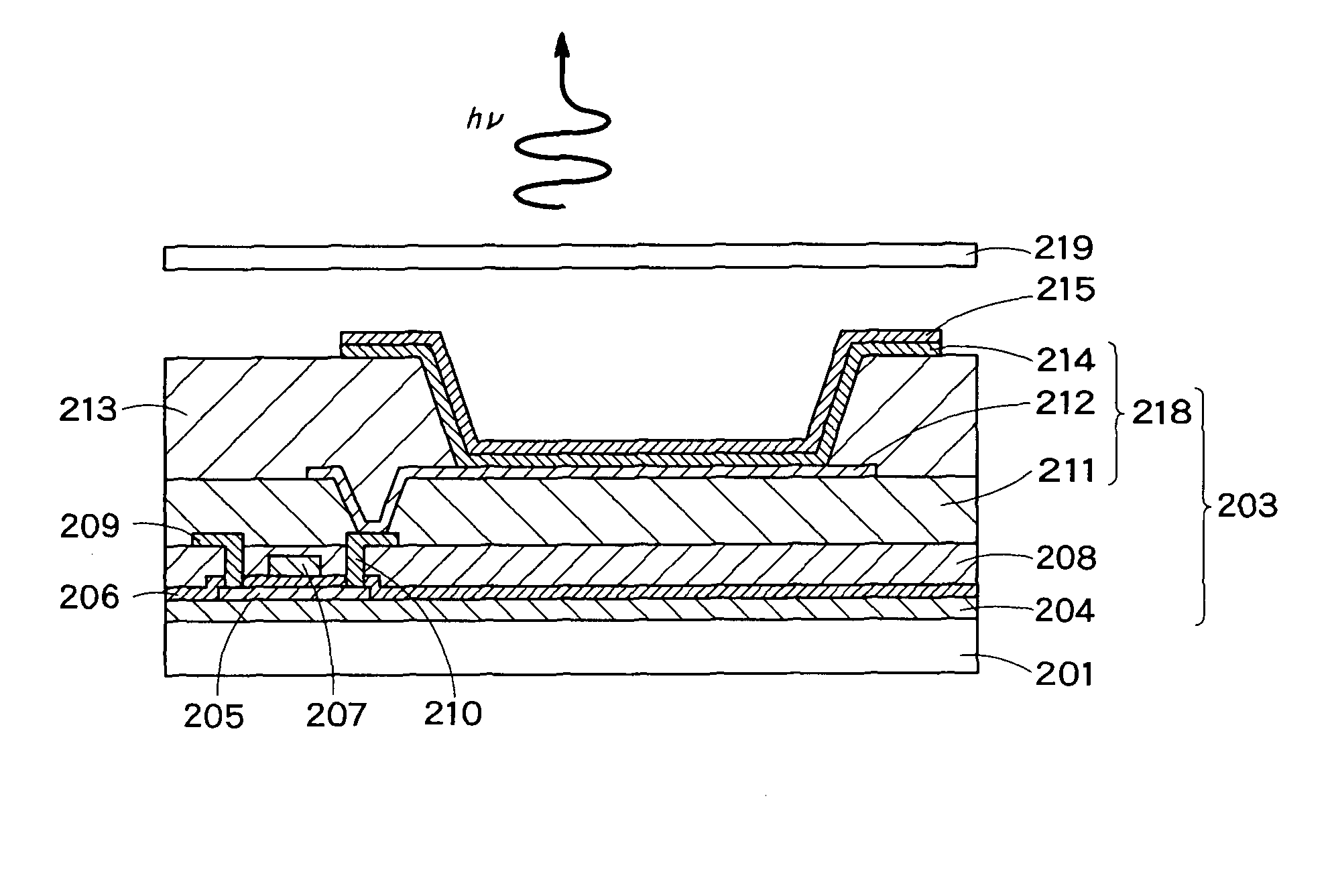
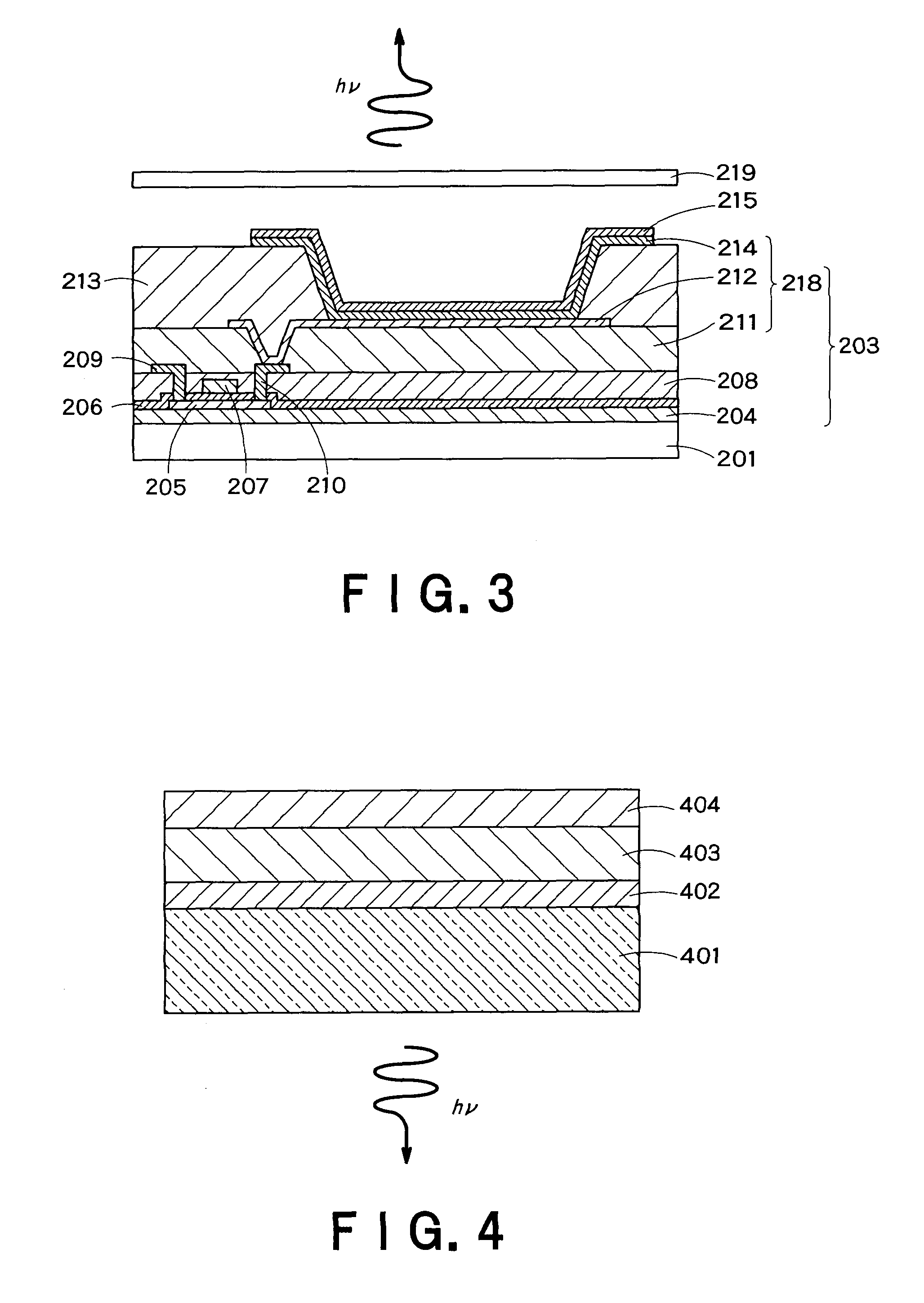
[0156]On a glass substrate, SiO2 and SiN were deposited by the plasma CVD method in thicknesses of 100 nm and 50 nm, respectively, to prepare an undercoating layer. Successively, amorphous silicon was deposited by the plasma CVD method in 50 nm thickness to form a semiconductor layer. After subjected to dehydrogenation annealing, the semiconductor layer was irradiated with excimer laser beams to crystallize the amorphous silicon and thereby to from polysilicon on the area where TFT was to be provided. The area was then dry-etched by photolithography to pattern the polysilicon. Thereafter, SiO2 was deposited to form a gate-insulating layer, and MoW was deposited thereon. The deposited layer was subjected to patterning, to form a gate electrode. After doping, SiO2 was deposited by the plasma CVD method to form an interlayer dielectrics layer. Contact holes to the source area and the drain area were formed by photolithography, and then a source electrode 209 and a drain electrode 210, ...

example 2

[0159]The procedures of Example 1 were repeated to form layers of the display up to the organic layer. After that, MgAg alloy was co-deposited by vacuum deposition at the deposition rate of 10:1 to prepare a MgAg alloy layer of 5 nm thickness. Thereafter, a positive-type photoresist (THMR IP3250 [trademark], manufactured by Tokyo Ohka Kogyou Co., Ltd.) was spin-coated to form a resist layer of 80 nm thickness, and then an organic spin-on glass (SOG) composition (OCD-T7 5500-T [trademark], manufactured by Tokyo Ohka Kogyou Co., Ltd.) was coated and baked to form a SOG layer of 20 nm thickness. Further, a block polymer composed of polystyrene (PS) (Mw: 78000):polymethylmethacrylate (PMMA) (Mw: 170000) and PMMA (Mw: 1500) were mixed in the weight ratio of 6:4 to prepare a polymer solution, which was then coated and annealed so that the phase-separation pattern of the block polymer was generated.

[0160]The phase-separated pattern was dry-etched by oxygen gas, to remove the PMMA phase. Th...

example 3

[0161]The procedures of Example 1 were repeated to form layers of the display up to the organic layer. After that, MgAg alloy was co-deposited by vacuum deposition at the deposition rate of 10:1 to prepare a MgAg alloy layer of 30 nm thickness. Thereafter, a positive-type photoresist (THMR IP3250 [trademark], manufactured by Tokyo Ohka Kogyou Co., Ltd.) was coated and baked to form a resist layer of 80 nm thickness, and then an organic spin-on glass (SOG) composition (OCD-T7 5500-T [trademark], manufactured by Tokyo Ohka Kogyou Co., Ltd.) was coated and baked to form a SOG layer of 20 nm thickness. Further, a block polymer composed of polystyrene (PS) (Mw: 78000):polymethylmethacrylate (PMMA) (Mw: 170000) and PMMA (Mw: 1500) were mixed in the weight ratio of 6:4 to prepare a polymer solution, which was then coated and annealed so that the phase-separation pattern of the block polymer was generated. The phase-separated pattern was dry-etched by oxygen gas, to remove the PMMA phase. T...


PUM


Abstract

The Present invention provides an organic EL display and a lighting device having high efficiency. The organic EL display comprises a substrate, a pixel-driving circuit unit, and pixels arranged in the form of a matrix on the substrate. The pixel comprises a light-emitting part, and the light-emitting part is composed of a first electrode placed near to the substrate, a second electrode placed far from the substrate, and at least one organic layer placed between the first and second electrodes. The second electrode has a metal electrode layer having a thickness of 10 nm to 200 nm, and the metal electrode layer comprises a metal part and plural openings penetrating through the layer. The metal part is seamless and formed of metal continuously connected without breaks between any points therein. The openings have an average opening diameter of 10 nm to 780 nm, and are arranged so periodically that the distribution of the arrangement is represented by a radial distribution function curve having a half-width of 5 nm to 300 nm.

Description

CROSS-REFERENCE TO RELATED APPLICATIONS[0001]This application is based upon and claims the benefit of priority from the prior Japanese Patent Applications No. 73144 / 2008, filed on Mar. 21, 2008; the entire contents of which are incorporated herein by reference.BACKGROUND OF THE INVENTION[0002]1. Field of the Invention[0003]The present invention relates to a displaying device and a lighting device employing an organic electroluminescence element (hereinafter, referred to as “organic EL element”) of high efficiency.[0004]2. Background Art[0005]An organic EL element is a light-emitting device in which electrons and positive holes are injected into an organic layer to emit light. Because of self-luminosity, it is characteristic of the organic EL element to give high contrast views and to have a very thin light-emitting part. Accordingly, it is being studied to use the organic EL elements in practical application to thin flat displaying devices and thin flat lighting devices. These devic...

Claims


Application Information

Patent Timeline
Patent Type & Authority Patents(United States)
IPC IPC(8): H01J1/46
CPCH01L51/5203H01L51/5234H01L2251/5315H10K50/805H10K50/828H10K2102/3026
Inventor FUJIMOTO, AKIRAASAKAWA, KOJINAKANISHI, TSUTOMUTSUTSUMI, EISHIKITAGAWA, RYOTA
Owner KK TOSHIBA
Why Eureka
Try Eureka