Semiconductive counter electrode for electrolytic current distribution control

a counter electrode and electrolytic current technology, applied in the field of electrolytic techniques, can solve the problems of limiting the range of usable or obtainable electrolytic resistivity, unable to enable difficult to achieve uniform electroplating of metal, etc., to achieve the effect of enhancing electrolytic current distribution and improving electrolytic current distribution

Active Publication Date: 2012-04-03
NOVELLUS SYSTEMS
View PDF40 Cites 16 Cited by
  • Summary
  • Abstract
  • Description
  • Claims
  • Application Information

AI Technical Summary

Benefits of technology

[0024]The invention helps to solve some of the problems mentioned above by providing systems, apparatuses and methods for electrochemical treatment of integrated circuit substrates and other workpieces. In particular, embodiments in accordance with the invention are utilized to enhance electrolytic current distribution control during electroplating of metal onto a substrate, and also during removal of metal from a substrate by anodic dissolution. Embodiments in accordance with the invention are particularly useful to enhance electrolytic current distribution during electrochemical treatment of a substrate surface having a thin conductive, but relatively resistive layer, such as a thin metal seed layer.

Problems solved by technology

Thus, thin resistive films pose extreme terminal effect difficulties.
In extreme cases, the scale of the potential differences within the metal film can be so great as to cause reaction at the wafer edge to occur at or near the electrochemical diffusion limit where a number of undesirable characteristics in the deposition can result (e.g., dendritic morphology), while simultaneously little or no reaction occurs at all at the inner regions of the wafer.
Unfortunately, typical organic additives cannot create surface polarization in excess of about 0.5 V. Thus, conventional uniformity-enhancing techniques cannot create polarization and related voltage drops required for very-thin-film seed plating, and hence cannot enable uniform electroplating of metal when the sheet resistances are large.
Furthermore, electrolyte composition is often determined by other plating factors, which can limit the range of usable or obtainable electrolyte resistivity.
The high-resistance electrolyte approach has limits and potentially several very significant problems: (1) the limited solubility of metal (e.g., copper) in higher pH baths without resorting to strong metal complexing (chelating) agents; (2) the (often associated) fact that a bath tends not to retain its film-morphology and feature-filling characteristics; (3) the added kinetic resistance associated with lower copper concentration is not favorable; and (4) a low mass-transfer-diffusion-limited plating rate.
For example, thinner seed layers can lead to greater potential differences between the center and edge of a wafer, and hence to large variations in current density during plating.
Additionally, it is known that poor seed-layer side-wall coverage leads to higher average resistivities for current traveling normal to the feature direction (for trenches), also leading to large current-density differences between the center and edge of a wafer.
Any change in conditions which increases seed layer resistivity or a seed layer's electrical path exacerbates the difficulty of achieving a uniform current distribution (required to maintain effectively uniformity of feature electrofilling across an entire wafer).
Unfortunately, these trends produce more challenging conditions for electrofilling and are not generally amenable to maintaining uniform current density across a wafer.
However, a thinner seed layer can cause the voltage drop within the seed layer to be greater and the current distribution across the wafer to become more non-uniform, which (if left uncompensated) leads to poor electrofilling uniformity across the wafer.
These approaches have some limitations associated with the processes and with physical properties of the materials.
Also, because the conductivity of a plating bath is tied to its ionic concentration and pH, a decrease in bath conductivity directly and negatively impacts the rate of plating and the morphology of the plated material.

Method used


Image

  • Semiconductive counter electrode for electrolytic current distribution control
  • Semiconductive counter electrode for electrolytic current distribution control
  • Semiconductive counter electrode for electrolytic current distribution control

Examples


example 1

[0147]A prophetic example of embodiments in accordance with the invention includes electroplating of copper metal onto the surface of a substrate wafer having a copper metal seed layer.

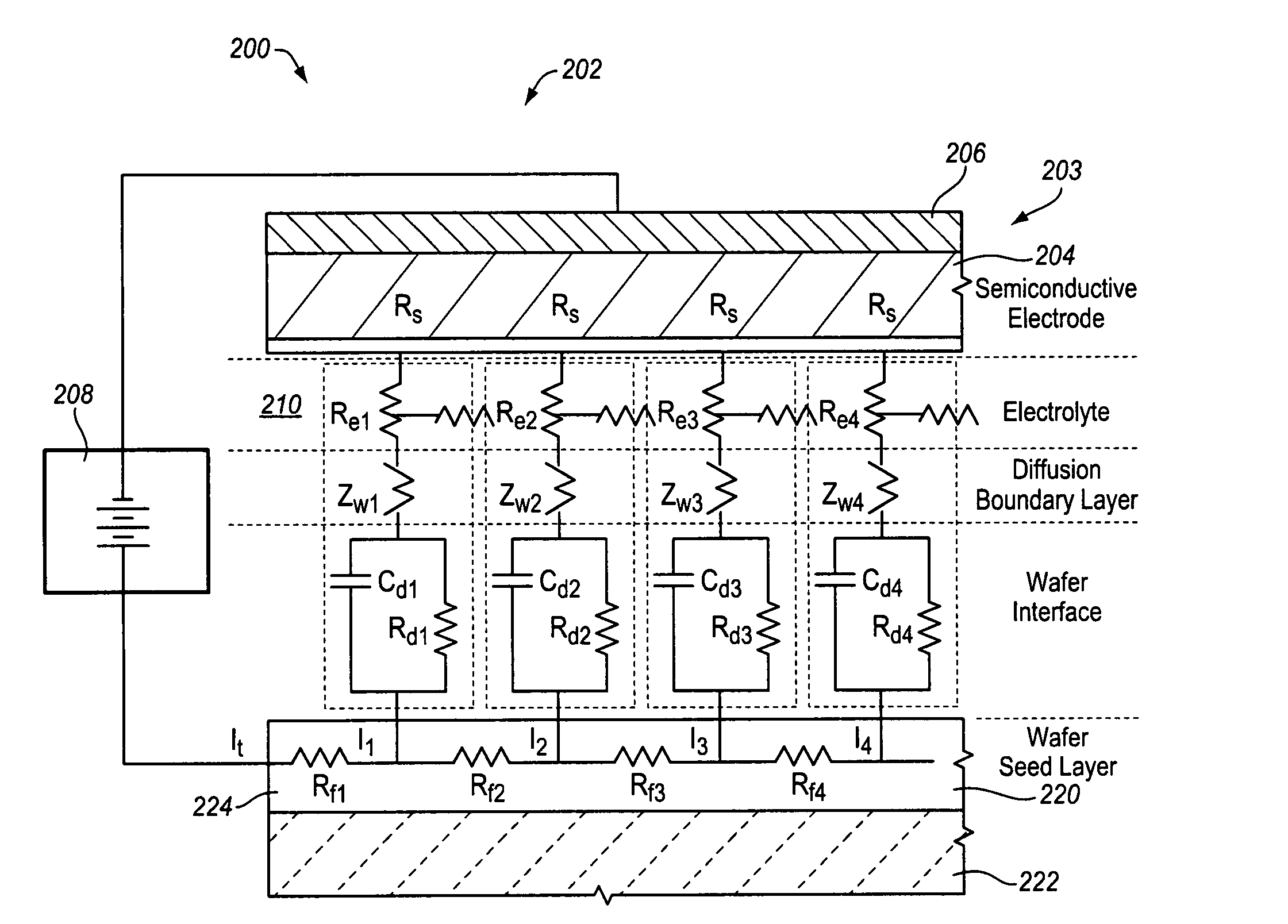
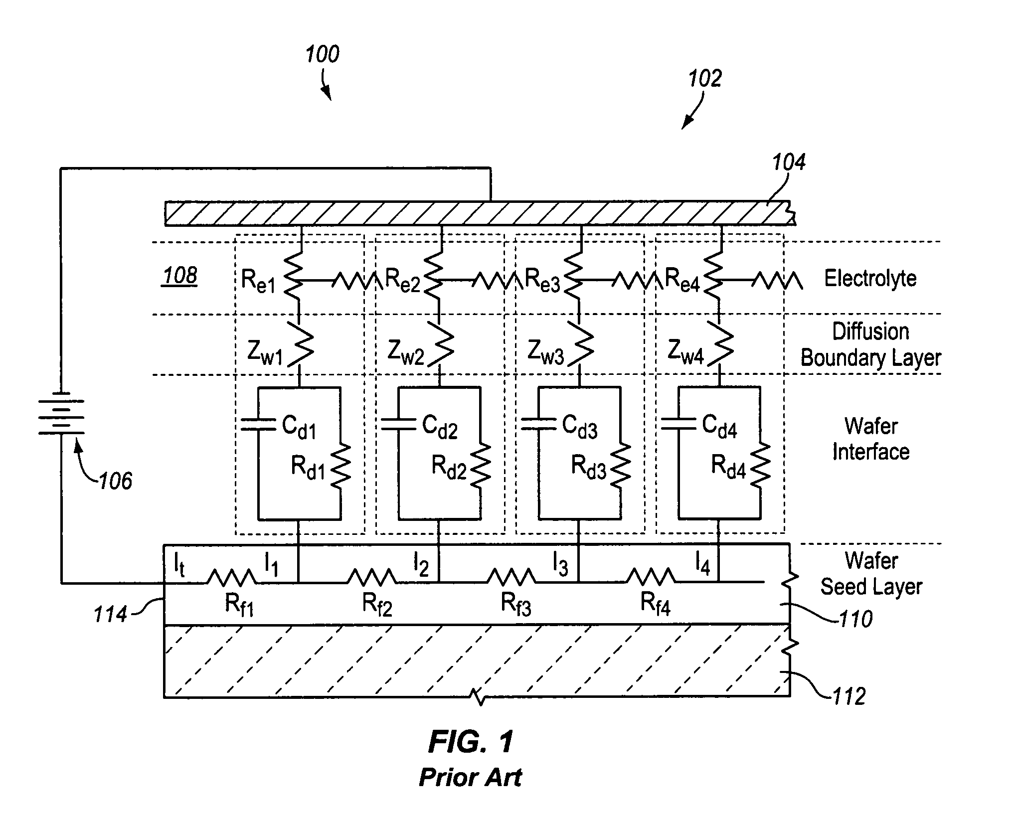
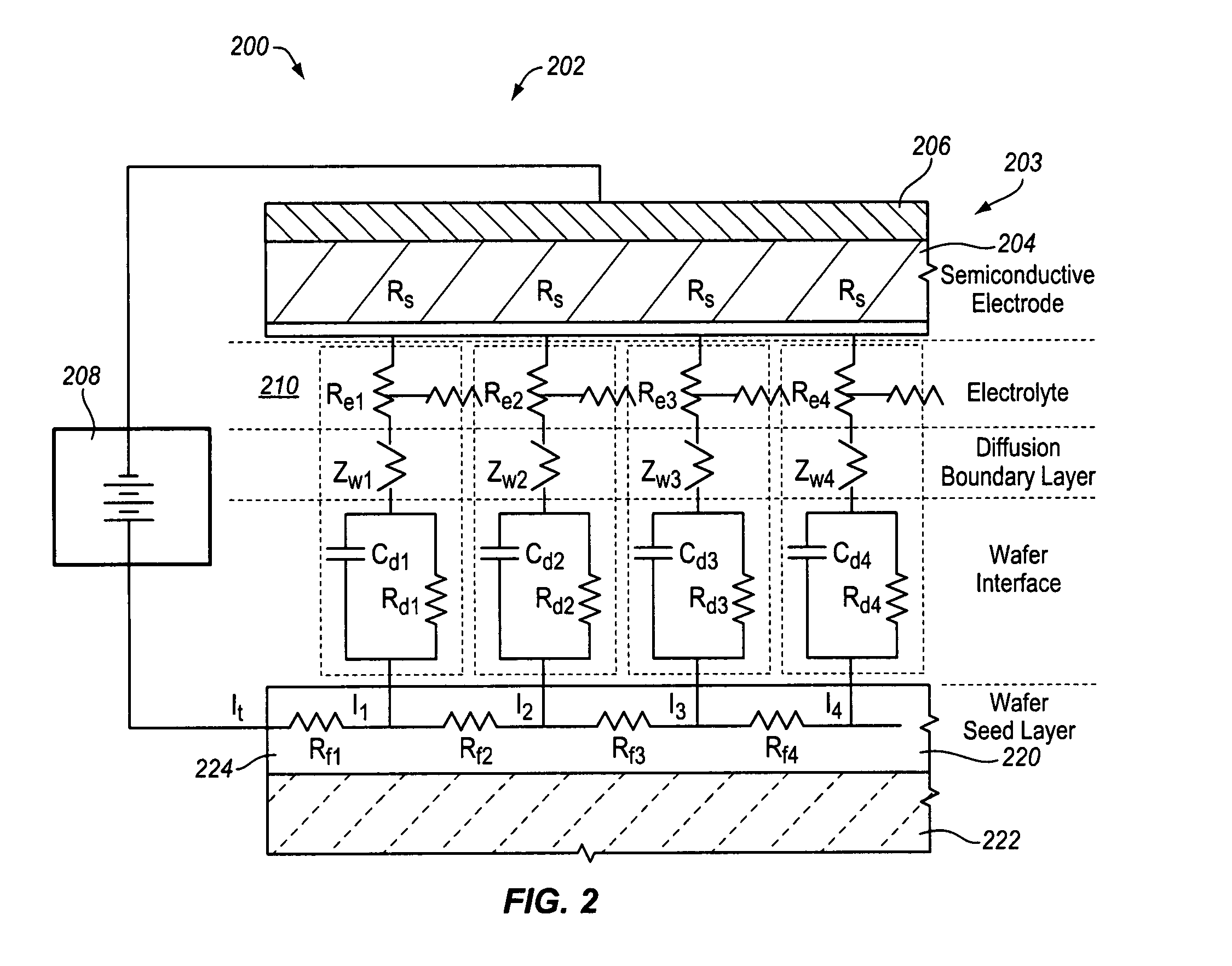
[0148]A plating bath container, such as treatment container 504 as depicted in FIG. 15, is filled with an electroplating solution comprising: 40 grams per liter (g / 1) of dissolved copper metal, added as copper sulfate pentahydrate (CuSO4.5H20); 10 g / l H2SO4; 50 milligrams per liter (mg / l) chloride ion, added as HCl; 6 milliliters per liter (ml / l) VIAFORM® accelerator; 2.5 ml / l VIAFORM® leveler; 2 ml / l (i.e., about 200 ppm) VIAFORM® suppressor. A semiconductive counter electrode assembly in accordance with the invention is located at the bottom of the plating bath container. The semiconductive counter electrode assembly comprises a cylindrical electric current buss and a semiconductive counter electrode (SCE). The SCE is mounted on and covers the cylindrical electric current buss. The SCE serves as a s...


PUM

PropertyMeasurementUnit
widthaaaaaaaaaa
thicknessaaaaaaaaaa
thicknessaaaaaaaaaa

Abstract

A semiconductive counter electrode covers a highly electronically conductive electric current buss. The semiconductive counter electrode is impervious to ion flow. A substrate holder is operable to hold a substrate and to form a thin fluid gap between the semiconductive counter electrode and a substrate surface. A thin liquid electrolyte layer is located in the thin fluid gap. A power supply connected to the electric current buss and a peripheral edge of a conductive substrate surface is able to generate a potential difference between the electric current buss and the semiconductive counter electrode, on one side of the electrolyte layer, and the substrate on the other side. The semiconductive counter electrode provides a substantial resistance in the various current flow paths between the electric current buss and the semiconductive counter electrode, on one side, and the conductive substrate surface, on the other, thereby enhancing control of current distribution.

Description

RELATED APPLICATIONS[0001]This application is a continuation in part application, claiming priority under 35 USC 120, of U.S. patent application Ser. No. 10 / 365,577, filed Feb. 11, 2003, by Steven T. Mayer et al., titled “Method And Apparatus For Potential Controlled Electroplating Of Fine Patterns On Semiconductor Wafers”.[0002]This application is also a continuation in part of U.S. patent application Ser. No. 11 / 040,359, filed Jan. 20, 2005, by Steven T. Mayer and Jonathan D. Reid, titled “High Resistance Ionic Current Source,” which claims the benefit under 35 USC 119(e) of U.S. Provisional Application No. 60 / 580,433, filed Jun. 16, 2004; and which is also a continuation in part of U.S. patent application Ser. No. 10 / 318,497, filed Dec. 11, 2002, by Steven T. Mayer et al., titled “Copper Electroplating Method And Apparatus”, now U.S. Pat. No. 6,890,416, and which is also a continuation in part of U.S. application Ser. No. 10 / 916,374, by Steven T. Mayer, filed Aug. 10, 2004, title...

Claims


Application Information

Patent Timeline
Patent Type & Authority Patents(United States)
IPC IPC(8): C25D17/10C25B9/00C25D5/00
CPCC25D17/10C25D17/12C25D21/12C25F7/00H01L21/2885C25D17/008C25D17/002C25D17/005C25D17/001C25D17/06H01L21/76877Y10S204/07
Inventor MAYER, STEVEN T.REID, JONATHAN D.
Owner NOVELLUS SYSTEMS
Why Eureka
Try Eureka