Ion sputter removal from thin microscopy samples with ions extracted from an RF generated plasma

a plasma and plasma technology, applied in the field of assembly, can solve the problems of preventing the achievement of the desired resolution, reducing affecting the quality of high resolution images, so as to improve the sputter removal rate and minimize or eliminate the sputter deposition of materials

Active Publication Date: 2012-10-16
TED PELLA
View PDF17 Cites 11 Cited by
  • Summary
  • Abstract
  • Description
  • Claims
  • Application Information

AI Technical Summary

Benefits of technology

[0014]The basis of this application is to configure a TEM sample to be plasma-trimmed in a geometry and orientation within the plasma to modify the trajectory of ions from the plasma to sample in order to enhance the sputter removal rate at low angles in order to remove the damaged region from the sample. The energy and the current of the ions can be reproducibly controlled by controlling the plasma processing parameters and the bias on the sample. Further, the geometry of...

Problems solved by technology

It is well known that the conventional methods of preparing TEM specimens produce artifacts that detract from the quality of high resolution images because of damage at the top and bottom of the sample.
With the specimen thickness requirements of the highest resolution instruments that can achieve sub-angstrom resolution, the surface artifacts can become an appreciable thickness fraction of the sample under observation and prevent the achievement of the desired resolution.
For example, mechanical polishing techniques to promote electron transparency, such as the tripod polishing technique or dimple grinding, will create surface scratches and subsurface damage in the form of amorphous regions and crystalline defects such as dislocations and dislocation loops and twinning, and can even cause re-crystallization or phase changes....

Method used


Image

  • Ion sputter removal from thin microscopy samples with ions extracted from an RF generated plasma
  • Ion sputter removal from thin microscopy samples with ions extracted from an RF generated plasma
  • Ion sputter removal from thin microscopy samples with ions extracted from an RF generated plasma

Examples


Embodiment Construction

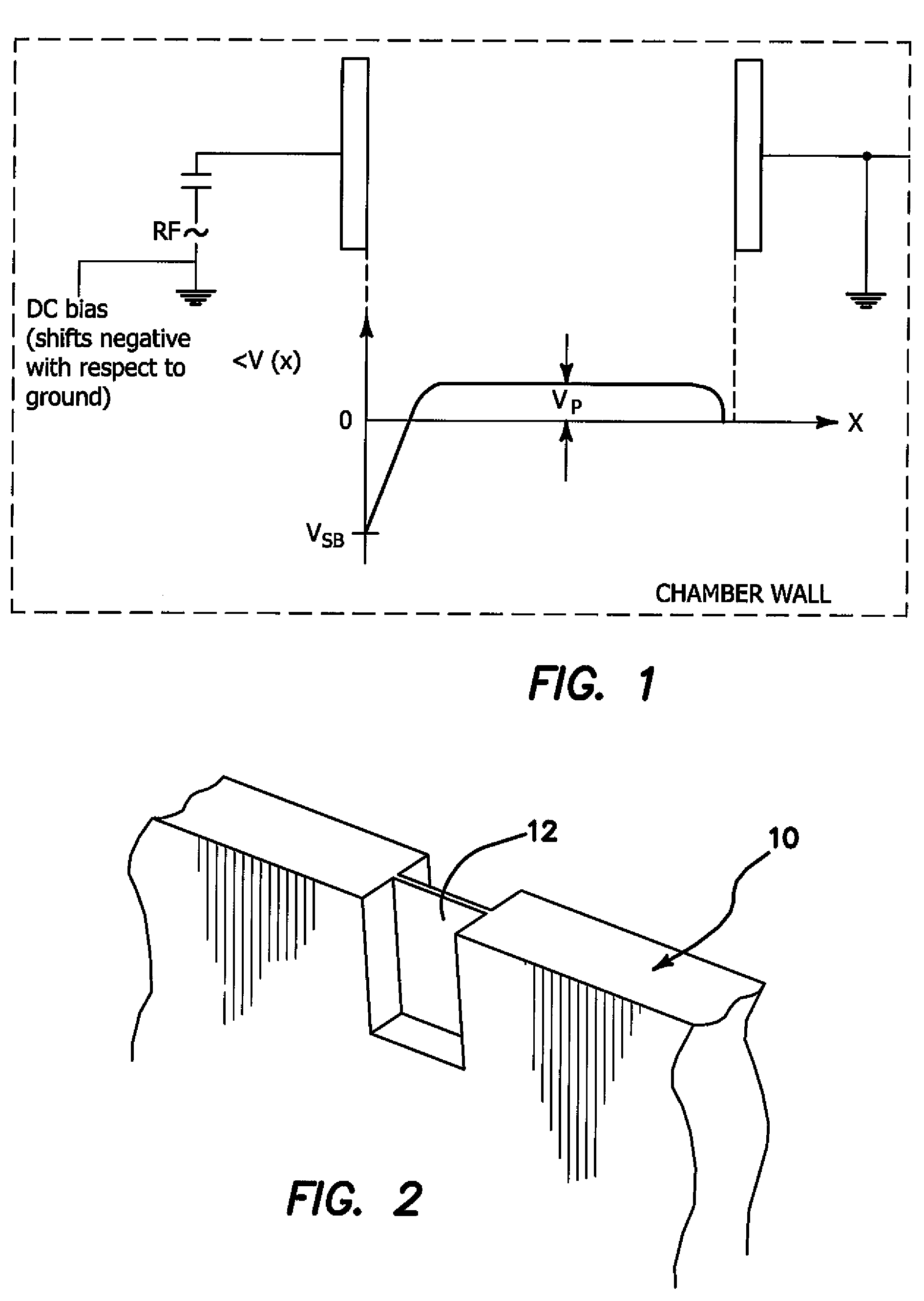
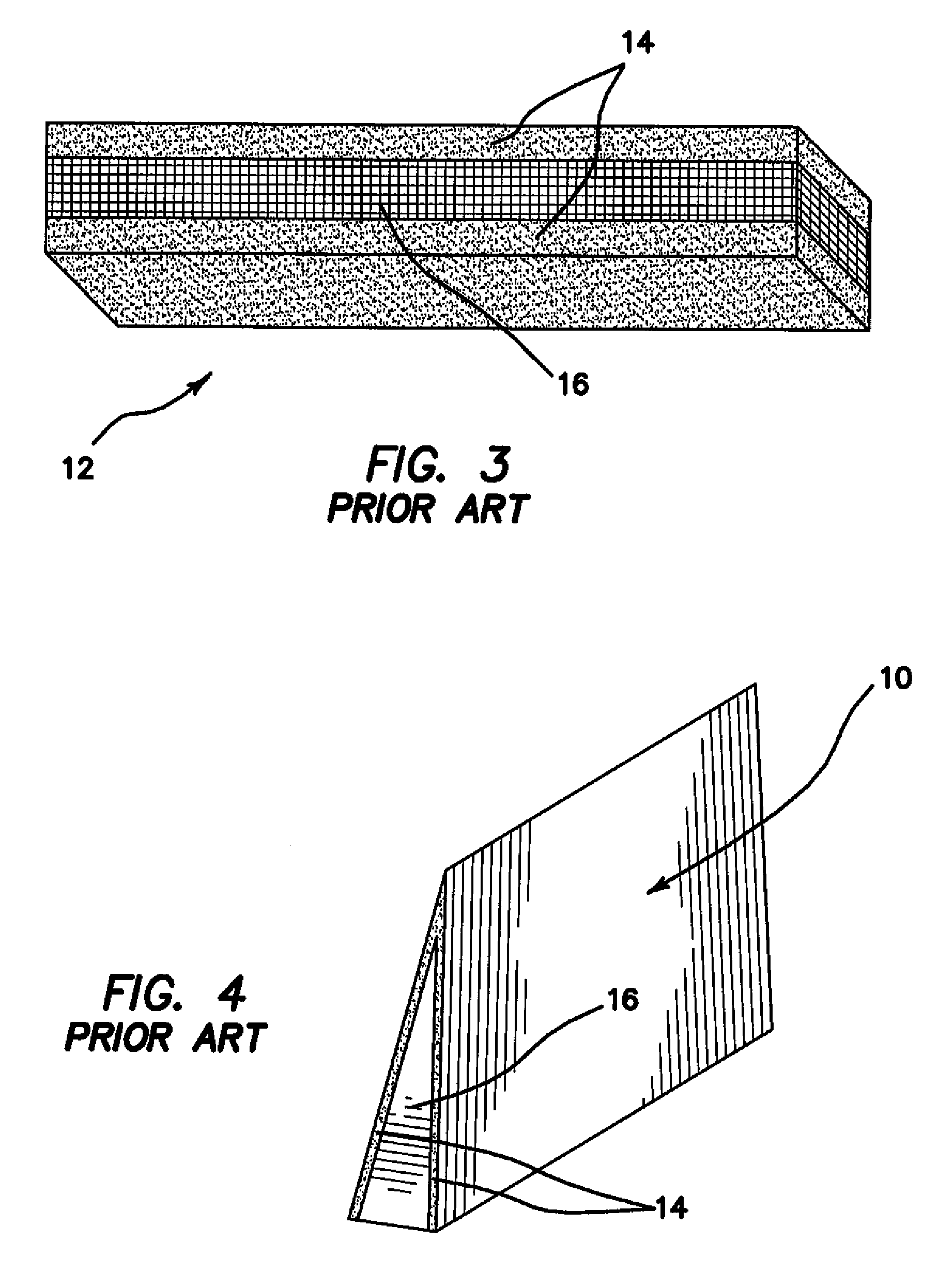
[0040]Referring now more particularly to the drawings, there is shown in FIG. 2 the geometry of a typical prior art “H-Bar” FIB prepared TEM material sample 10. A thin membrane 12 in the center portion of the sample 10 is electron transparent because its thickness typically varies between approximately 20 and 200 nm. This membrane 12 is the “H-Bar” cut membrane portion of the sample 10 which is used as the TEM sample. FIG. 3 illustrates a representative parallel-sided membrane 12, which has been cut with a FIB. Both sidewalls of the membrane 12, which comprise the top and bottom of the TEM sample as it appears in a microscope, can have a thickness of up to 23 nm of an amorphous thickness layer 14 below each surface. An undamaged portion 16 of the sample is the only region representative in the microscope of the original starting material.

[0041]Referring now to FIG. 4, there is shown a schematic representation of a tapered prior art TEM sample 10 that might be prepared by ion milling...


PUM


Abstract

A plasma system for changing a microscopy material sample comprises a microscopy material sample holder for holding a microscopy material sample in place in a desired orientation, and a receptacle holder for receiving the sample holder and an RF antenna. The microscopy sample is positioned relative to the antenna so that no point on the antenna is in direct line-of-sight contact with the microscopy sample. This feature of avoiding direct line-of-sight contact between the antenna and the sample assists in preventing, or at least minimizing, ion sputtering of system component material onto the specimen or sample 10 that is being trimmed. Moreover, portions of the system which are in direct line-of-sight contact with the sample are comprised of material having a low sputtering yield, preferably carbon. The material may comprise graphite, and may be in the form of a carbon coating or a carbon paint.

Description

[0001]This application claims the benefit under 35 U.S.C. 119(e) of the filing date of Provisional U.S. Application Ser. No. 60 / 926,052, entitled Methods & Systems for the Low Energy and Low Angle Ion Sputter Removal of Material from Thin Microscopy Samples with Ions Extracted from an RF Generated Plasma, filed on Apr. 23, 2007, which application is expressly and entirely incorporated herein by reference.[0002]Additionally, this application is related to commonly assigned U.S. application Ser. No. 11 / 712,830, entitled Reusable Holder for Transmission Electron Microscopy (TEM), Scanning Electron Microscopy (SEM), and Focused Ion Beam (FIB) Samples, filed on Feb. 28, 2007 and presently pending, which application is expressly and entirely incorporated herein by reference.BACKGROUND OF THE INVENTION[0003]This invention generally relates to assemblies for holding material specimens, and more particularly relates to a specimen holder and mating receptacle holder arrangement for a plasma s...

Claims


Application Information

Patent Timeline
IPC IPC(8): G21K5/08
CPCH01J37/32082H01J37/20H01J2237/31745H01J2237/2007
Inventor WALCK, SCOTT D.
Owner TED PELLA
Why Eureka
Try Eureka