Ion source and plasma processing apparatus

a plasma processing apparatus and inductive coupling technology, applied in the direction of plasma technique, vacuum evaporation coating, coating, etc., can solve the problems of increased dielectric loss, increased dielectric loss, difficulty in stable formation or maintenance of plasma, etc., and achieve the effect of reducing the dielectric loss between the high-frequency antenna and the plasma generating chamber and stably forming

Active Publication Date: 2013-01-22
UI VAC
View PDF13 Cites 33 Cited by
  • Summary
  • Abstract
  • Description
  • Claims
  • Application Information

AI Technical Summary

Benefits of technology

[0021]According to this invention, the dielectric loss between the high-frequency antenna and the plasma generating chamber can be reduced and the plasma can be stably formed and maintained for a prolonged period.

Problems solved by technology

As a result, a dielectric loss is increased.
As described above, when the conductive materials adhere on the inner peripheral surface of the partition wall 2 around the whole periphery thereof, the dielectric loss is increased and also high-frequency power for obtaining a desired plasma density is increased, thereby finally causing the problem of difficulty in stable formation or maintenance of plasma.

Method used


Image

  • Ion source and plasma processing apparatus
  • Ion source and plasma processing apparatus
  • Ion source and plasma processing apparatus

Examples


first embodiment

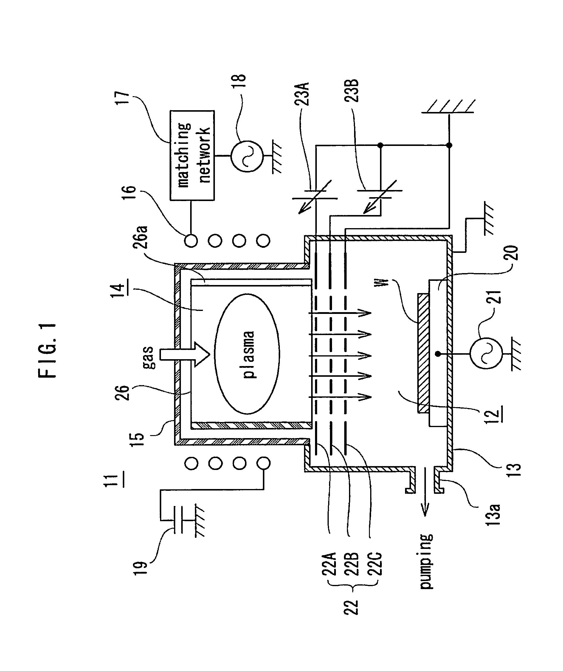
[0061]FIG. 1 is a schematic view of a plasma processing apparatus 11 having an ion source according to a first embodiment of this invention. The plasma processing apparatus 11 of this embodiment includes a vacuum chamber 13 containing a processing chamber 12. The processing chamber 12 accommodates a substrate to be processed (hereinafter, simply referred to as “substrate”) W such as a semiconductor wafer or a substrate for a liquid crystal panel. The vacuum chamber 13 has an evacuation pipe 13a communicating with vacuum evacuation means (not shown) such as vacuum pumps. Therefore, the inside of the processing chamber 12 can be depressurized to a predetermined vacuum level.

[0062]A partition wall 15 is installed at the upper portion of the vacuum chamber 13. The partition wall 15 partitions a plasma generating chamber communicated with the processing chamber 12. The partition wall 15 is made of a dielectric material such as quartz (a quartz bell jar?). A high-frequency antenna 16 woun...

second embodiment

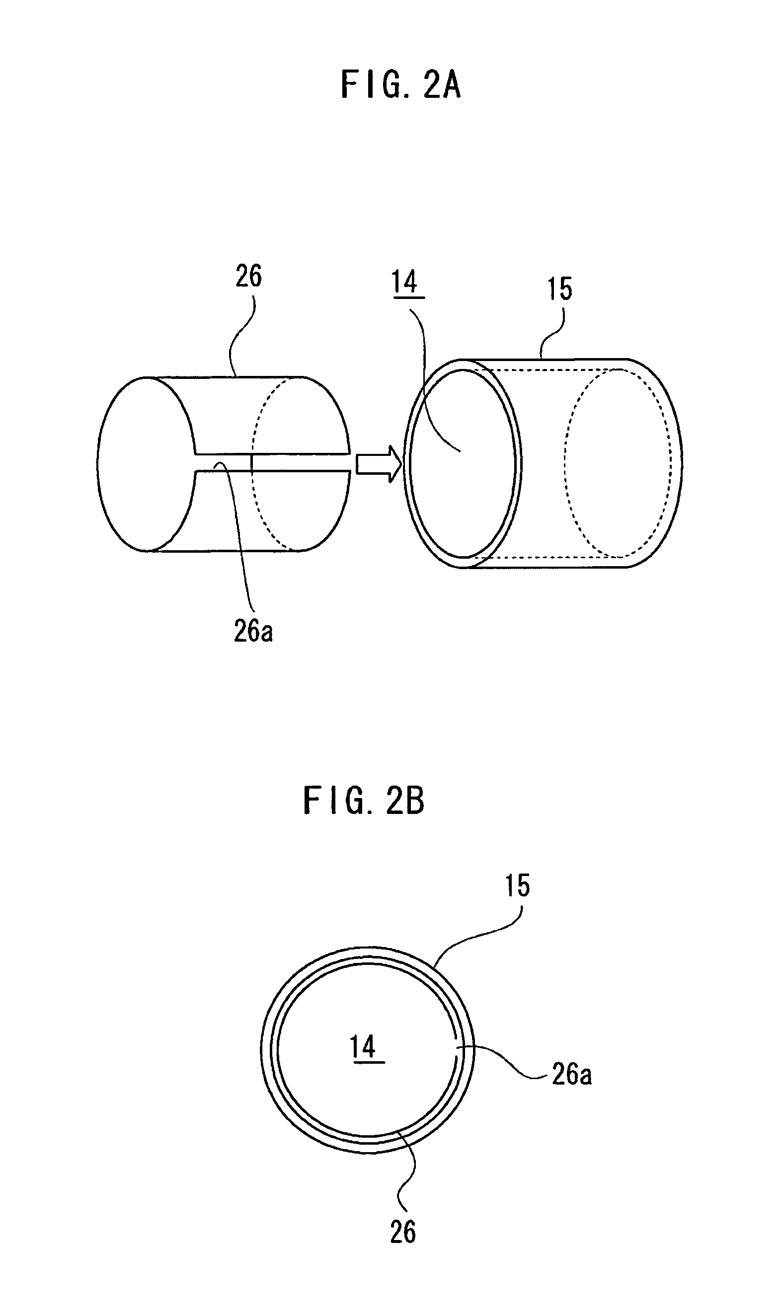
[0083]Then subsequently, FIGS. 5 and 6 show other embodiments of “the structure” pertaining to this invention. Parts that correspond to those in the above first embodiment are denoted by the same reference numerals. Therefore the detailed description of these parts will be omitted.

[0084]In the embodiment shown in FIGS. 5A and 5B, projections 15a extended in the direction crossing the winding direction of the high-frequency antenna 16 (FIG. 1) are provided. The projections 15a are formed on the inner peripheral surface of the cylindrical partition wall 15 partitioning the plasma generating chamber 14. According to this construction, sputtered materials are prevented from depositing onto the inner surface of the partition wall 15 in series in the peripheral direction thereof by the projections 15a. Therefore, the dielectric loss of the high-frequency antenna 16 can be reduced.

[0085]When the sputtered materials adhere onto both sides of the projection 15a, a direction of the current fl...

third embodiment

[0093]FIGS. 7 and 8 show a third embodiment of this invention. Parts that correspond to those in the above first and second embodiments are denoted by the same reference numerals. The detailed description of these parts will be omitted.

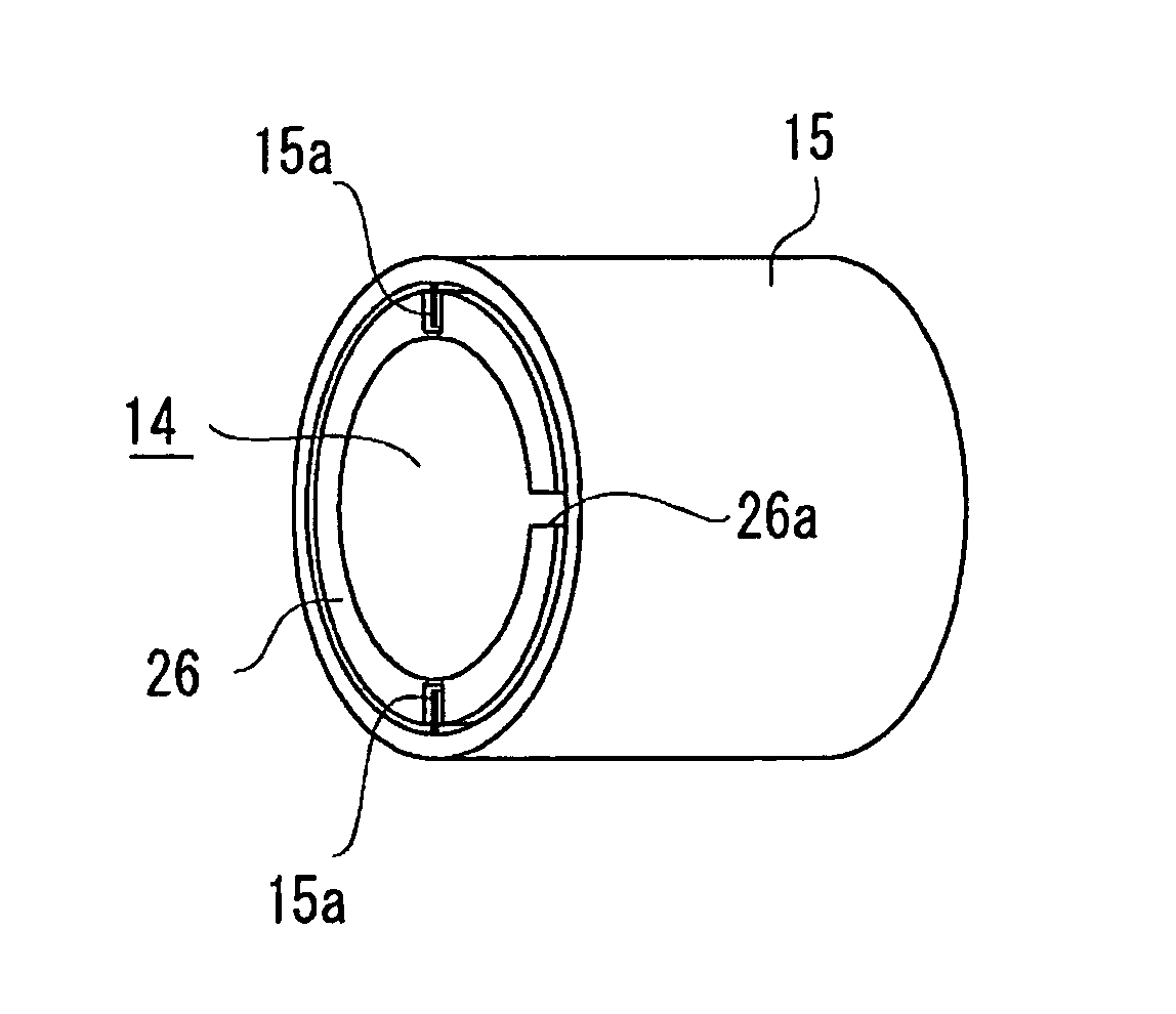
[0094]In this embodiment, a structure is provided in which the shield body 26 described in the first embodiment and the inner surface structure of the partition wall 15 described in the second embodiment are combined.

[0095]In the embodiment shown in FIGS. 7A and 7B, the recesses 15b are formed on the inner peripheral surface of the cylindrical partition wall 15 partitioning the plasma generating chamber 14. The recesses 15b are extended in the direction crossing the winding direction of the high-frequency antenna 16 (FIG. 1). Further, the shield body 26 is made of a dielectric material and is installed inside the partition wall 15. The slot 26a is formed at the shield body 26 in the direction crossing the winding direction of the high-frequency antenn...


PUM

PropertyMeasurementUnit
frequencyaaaaaaaaaa
gas pressureaaaaaaaaaa
widthaaaaaaaaaa

Abstract

It is an object of this invention to provide an ion source and a plasma processing apparatus capable of generating stable and long-life plasma. The ion source is provided with a high-frequency antenna (16) installed on the outer peripheral side of a partition wall (15) made of a dielectric material and partitioning a plasma generating chamber (14) and a shield body (26) made of a dielectric material and preventing deposition on the inner peripheral surface of the partition wall (15) facing the high-frequency antenna (16) inside the plasma generating chamber (14). The structure made of a dielectric material can prevent an increase in high-frequency power required for inductive coupling with plasma. The shield body (26) is formed with a slot (26a) in a direction crossing a winding direction of the high-frequency antenna (16). Since this arrangement can prevent continuous deposition on the inner surface of the partition wall in the winding direction of the high-frequency antenna, an induction loss between the high-frequency antenna and the plasma generating chamber can be effectively prevented even if the deposited film is made of a conductive material.

Description

TECHNICAL FIELD[0001]This invention relates to an ion source of the inductive coupling type and a plasma processing apparatus having the same, and more particularly to an ion source and a plasma processing apparatus in which stable generation or maintenance of plasma is enabled by restraining deposition or adhesion on the inner surface of a partition wall that partitions a plasma generating chamber.BACKGROUND ART[0002]Conventionally, a plasma process is utilized for manufacturing semiconductors and electronic devices or for surface modification of structural materials. Examples of these kinds of plasma processes include ion beam etching and ion beam sputtering. Ion beam etching is the etching process of extracting ions from plasma in the form of a beam and then irradiating a metal film on the surface of a substrate to be processed with the ions. The ion beam sputtering is the sputtering process of extracting ions from plasma in the form of a beam, irradiating a sputtering target wit...

Claims


Application Information

Patent Timeline
Patent Type & Authority Patents(United States)
IPC IPC(8): C23C16/00
CPCH01J37/3053H01J37/32357H01J37/32422H05H1/46H01J2237/022H01J2237/08H01J2237/16H01J2237/0213H01J37/08H01J37/32H01J37/317
Inventor SASAKI, NARUYASUSHIMIZU, SABUROUKUNIBE, TOSHIJU
Owner UI VAC
Why Eureka
Try Eureka