
Silicon-based thin film solar cell and method for manufacturing same

a thin film solar cell and silicon-based technology, applied in the direction of solid-state devices, pv power plants, semiconductor devices, etc., can solve the problems of increasing the thickness of the layer, increasing the cost and time and increasing the short-circuit current of the solar cell, so as to suppress the recombination of carriers, improve the electron collecting effect, and reduce the cost of depositing the layer

Inactive Publication Date: 2013-09-10
KANEKA CORP
View PDF15 Cites 0 Cited by
  • Summary
  • Abstract
  • Description
  • Claims
  • Application Information

AI Technical Summary

Benefits of technology

The present invention relates to a solar cell design that improves its performance. Specifically, it includes a layer of n-type silicon alloy that acts as an electron collector and has a wide gap to improve the open circuit voltage of the solar cell. The n-type silicon alloy layer also prevents recombination of carriers by repelling holes. Additionally, a layer of n-type amorphous silicon is deposited on the n-type silicon alloy layer, which acts as an underlayer for the amorphous silicon layer and prevents crystallization by a different element such as oxygen, carbon, or nitrogen. This results in a thin-film solar cell with higher conversion efficiency.

Problems solved by technology

While the photoelectric conversion layer preferably has a larger thickness for its better light absorption, an excessive increase of the thickness inevitably increases cost and time for depositing the layer.
One of the big challenges in mass production of the thin film solar cell is high-speed film formation of the crystalline i-type silicon photoelectric conversion layer of the crystalline silicon photoelectric conversion unit performed by a CVD method with in-plane uniformity.
On the other hand, although discharge is performed on conditions of high pressure, high hydrogen dilution and high output with an interelectrode distance being in a narrowed state for the high-speed film formation of crystalline silicon (e.g., Patent Document 1, Non-patent Document 1 and Non-patent Document 2), grain boundaries of microcrystalline silicon are prone to be generated and defects are prone to be concentrated on the crystal grain boundaries under the high-speed film formation conditions, thereby causing a problem that a fill factor and an open circuit voltage of the solar cell are prone to decrease.
However, when the dilution ratio of hydrogen is decreased, the crystal volume fraction tends to decrease and become non-uniform, leading to a decrease in short-circuit current of the solar cell.
Further, the crystalline silicon photoelectric conversion unit with a low crystal volume fraction also has a problem of being sensitive to photodegradation.
Meanwhile, although the film thickness of the photoelectric conversion layer is preferably large in order to increase light absorption by the i-type layer so as to enhance the photoelectric conversion efficiency of the solar cell, when the film thickness of the i-type layer is made larger than necessary, the cost and the time for the film formation increases.

Method used

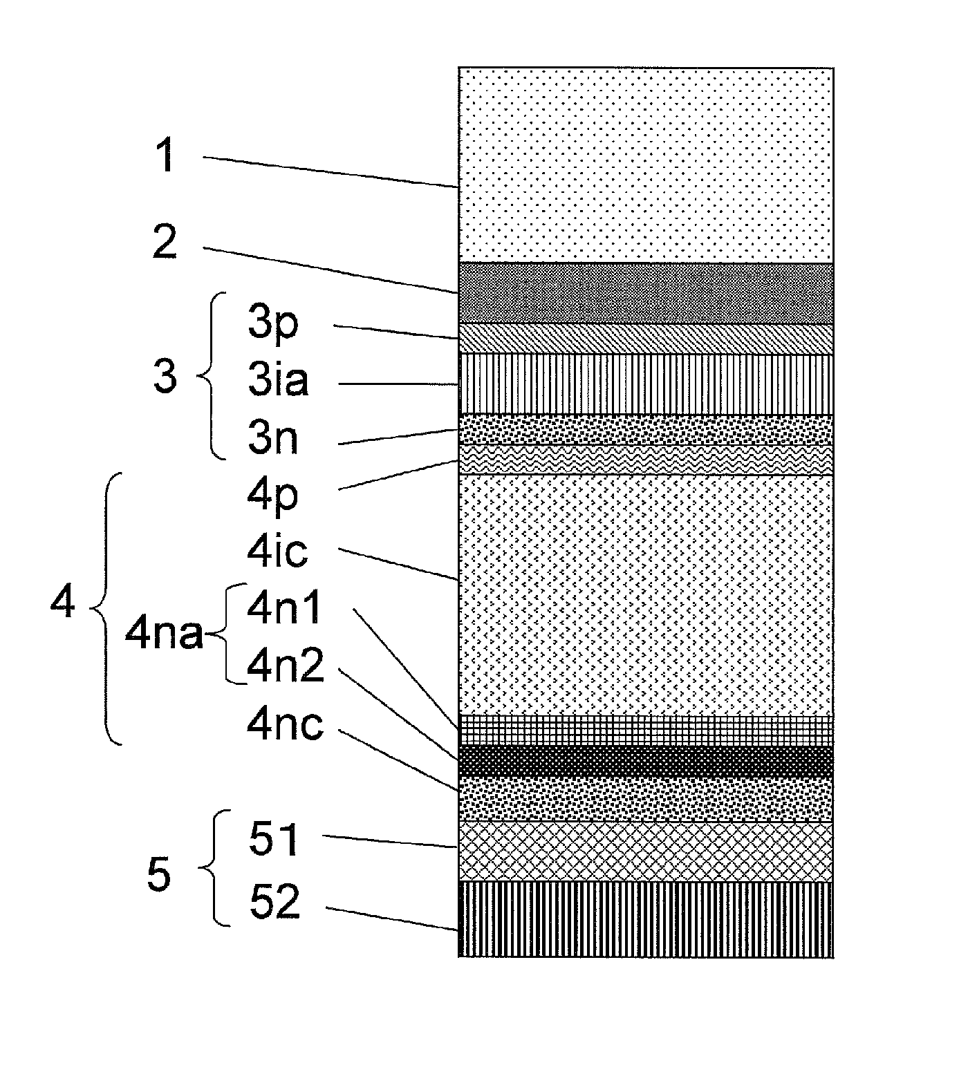
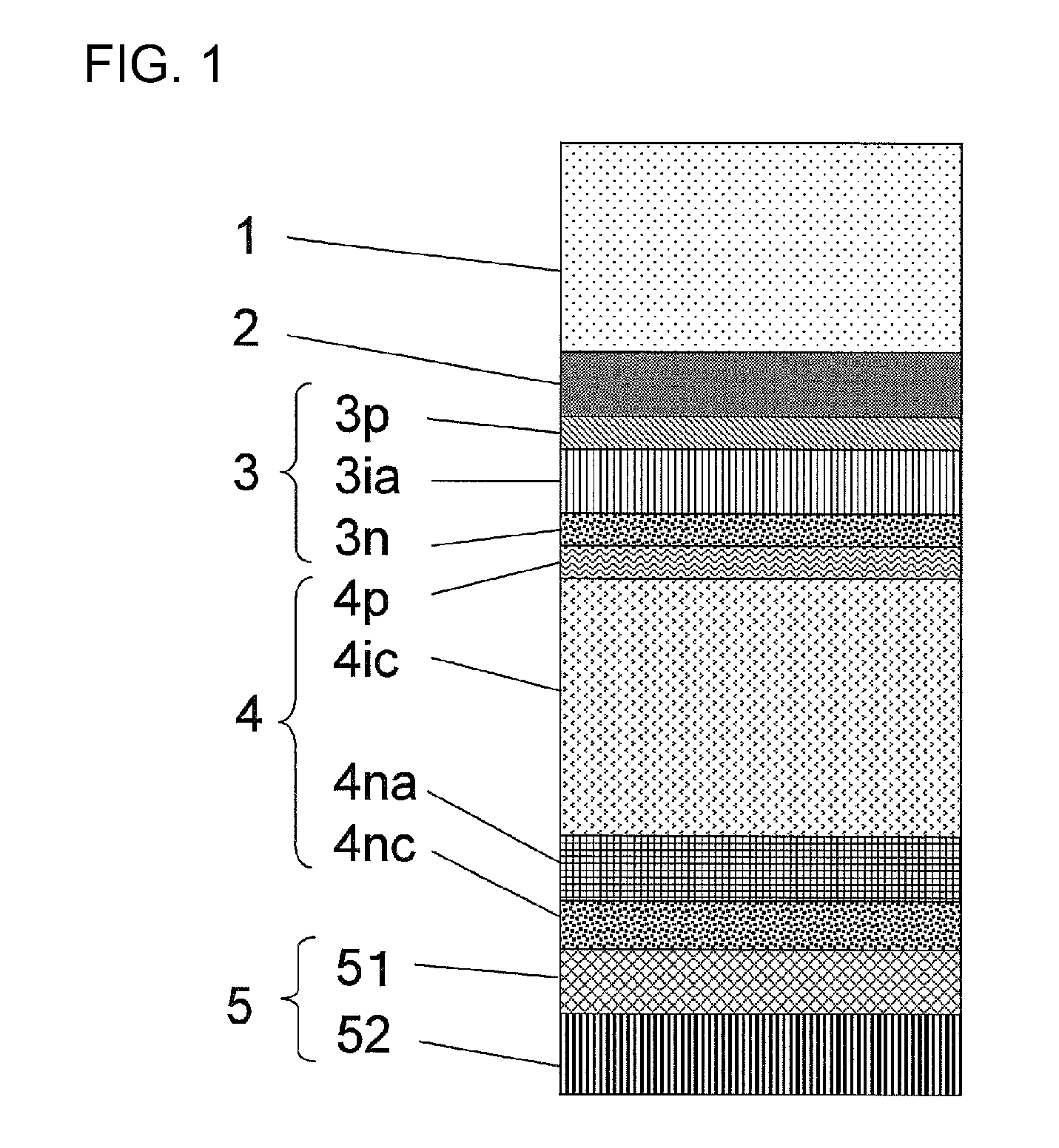

Image

  • Silicon-based thin film solar cell and method for manufacturing same
  • Silicon-based thin film solar cell and method for manufacturing same
  • Silicon-based thin film solar cell and method for manufacturing same

Examples


example 1-1

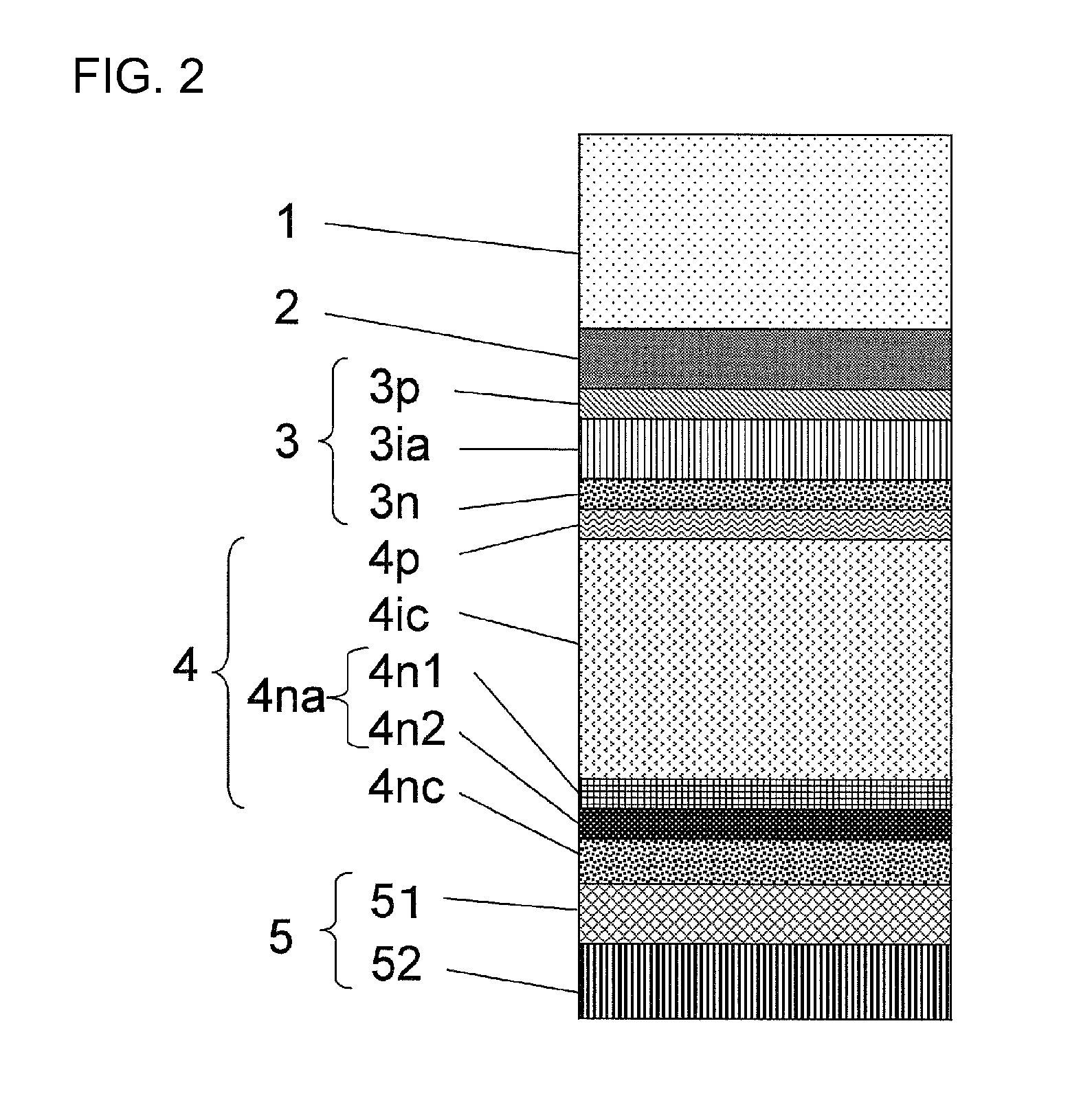
[0092]In Example 1-1, the hybrid silicon-based thin film solar cell schematically shown in FIG. 2 was produced in accordance with the following procedure.

[0093]First, on one principal surface of the transparent substrate 1 made of a glass substrate with a thickness of 1.1 mm, the transparent conductive film 2 made of SnO2 and having a fine roughness structure on its surface was formed by a thermal CVD method.

[0094]Next, in order to form the amorphous silicon photoelectric conversion unit 3, the transparent substrate1 with the transparent conductive film 2 formed thereon was introduced into a high-frequency plasma enhanced CVD apparatus and heated to 160° C., and thereafter, the amorphous p-type silicon carbide layer 3p with a thickness of 15 nm, the non-doped amorphous i-type silicon photoelectric conversion layer 3ia with a thickness of 300 nm, and the n-type silicon layer 3n with a thickness of 30 nm were sequentially disposed.

[0095]Further, in order to form the crystalline silico...

example 1-2

[0102]A hybrid silicon-based thin film solar cell was produced according to Example 1-1, with a difference from Example 1-1 in that in Example 1-2, the n-type amorphous silicon layer 4n2 was not formed and the n-type amorphous silicon carbide layer 4n1 was formed to have a film thickness of 8 nm.

example 1-3

[0103]A hybrid silicon-based thin film solar cell was produced according to Example 1-1, with a difference from Example 1-1 in that in Example 1-3, the n-type microcrystalline silicon oxide layer 4n1 was formed as the n-type silicon alloy layer to have a film thickness of 3 nm in place of forming the n-type amorphous silicon carbide layer 4n1 to have a film thickness of 3 nm. Film formation conditions for the n-type microcrystalline silicon oxide layer 4n1 in Example 1-3 were: a distance between the substrate surface for film formation and the electrode of 8 mm, a pressure of 1100 Pa, a plasma output of 0.16 W / cm2, and a SiH4 / PH3 / H2 / CO2 flow ratio of 1 / 6 / 200 / 4.


PUM

PropertyMeasurementUnit
thicknessaaaaaaaaaa
pressureaaaaaaaaaa
temperatureaaaaaaaaaa

Abstract

A method for manufacturing a silicon-based thin film solar cell including a crystalline silicon photoelectric conversion unit which contains a p-type layer (4p), a crystalline i-type silicon photoelectric conversion layer (4ic), and an n-type layer (4nc) stacked in this order from a transparent substrate side is provided. In one example, an n-type silicon-based thin film layer (4na) is formed on the crystalline i-type silicon photoelectric conversion layer (4ic), the n-type silicon-based thin film layer (4na) having an n-type silicon alloy layer having a film thickness of 1-12 nm and being in contact with the crystalline i-type silicon photoelectric conversion layer.

Description

TECHNICAL FIELD[0001]The invention relates to a silicon-based thin film solar cell and a method for manufacturing thereof. Particularly, the invention relates to a hybrid silicon-based thin film solar cell including an amorphous silicon photoelectric conversion unit and a crystalline silicon photoelectric conversion unit, in this order from a light incident side, and a method for manufacturing thereof.BACKGROUND ART[0002]In recent years, for realization of both lower cost and higher efficiency of a solar cell, a thin film solar cell, which is made using a small amount of raw materials, has attracted attention and is under intense development. Currently, in addition to a conventional amorphous thin film solar cell, a crystalline silicon thin film solar cell has also been developed, and a stacked solar cell, formed by stacking these cells and called a hybrid solar cell, has also been put into practical use. “Crystalline silicon” or “microcrystalline silicon” is a mixed crystal system ...

Claims


Application Information

Patent Timeline
Patent Type & Authority Patents(United States)
IPC IPC(8): H01L21/00H01L31/076H01L31/077H01L31/078
CPCH01L31/076H01L31/077H01L31/078Y02E10/548Y02E10/547
Inventor YOSHIKAWA, KUNTAICHIKAWA, MITSURUYAMAMOTO, KENJI
Owner KANEKA CORP
Learn More