IR detector

a detector and infrared technology, applied in the field of infrared detectors, can solve the problems of large increase in voltage difference across the thermopile, need biased voltage or current, and high cost of fabrication methods, so as to achieve high ir emissivity, improve performance, and high emissivity

Active Publication Date: 2013-10-08
AMS SENSORS UK LTD
View PDF17 Cites 57 Cited by
  • Summary
  • Abstract
  • Description
  • Claims
  • Application Information

AI Technical Summary

Benefits of technology

[0042]To improve the performance, the IR source may also have a material with high emissivity such as carbon nanotubes, carbon black, graphene, polyimide, a polymer, metal films, metal blacks, thin film stacks or other materials with high IR emissivity deposited or grown on the top of the membrane.
[0043]Alternatively the IR emissivity in the integrated IR source can be increased by etching selectively the CMOS metal layers above the silicon in a mesh shape or in a dot shape. The mesh size or the size of the dots and the distance of the dots is adjusted to increase the optical power at a particular wavelength and / or to filter out signal at other wavelengths. The etching of the metal layers above the silicon is done in the CMOS sequence, and therefore does not come with additional cost.

Problems solved by technology

The Seebeck effect causes a slight voltage difference across each thermocouple—resulting in a much large increase in voltage difference across the thermopile which is the sum of the voltages across each thermocouple.
However, these are formed by waferbonding of a P-type wafer and an N-type wafer and is also not specifically for use as an IR detector.
The fabrication method is also very expensive.
However, thermodiodes have the disadvantage that they need a biased voltage or current—which requires power.
In addition, it has a high base voltage, which makes it harder to measure small changes in the output voltage.
This will lead to high power consumption and lower maximum temperature of operation.
Moreover, the optical path is relatively small for the IR emission to travel, and so the sensor has a lower sensitivity.

Method used


Image

  • IR detector
  • IR detector
  • IR detector

Examples


Embodiment Construction

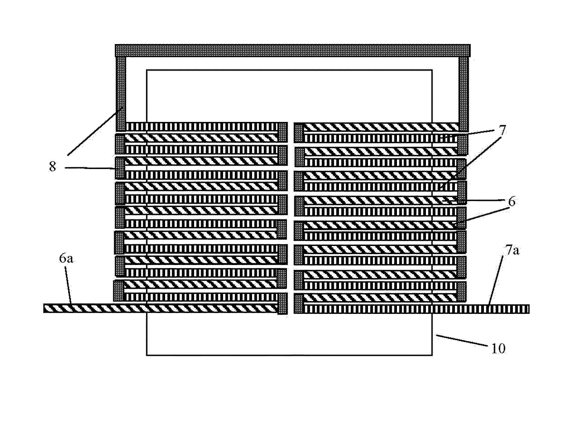
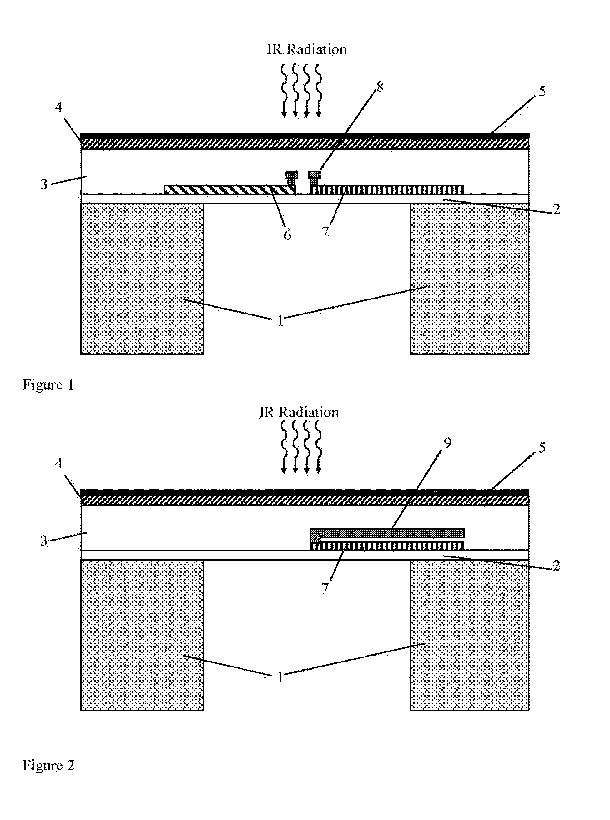
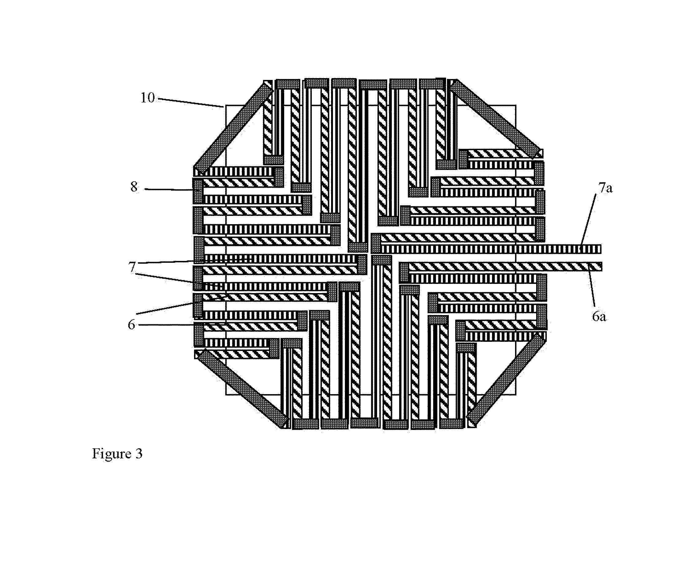
[0071]FIG. 1 shows a schematic cross section of an IR detector made in SOI process. There is provided a membrane layer 2,3,4 which is supported on a silicon substrate 1. The membrane layer includes a buried oxide layer 2, dielectric layers 3 and a passivation layer 4. A thermopile is formed within the membrane layer consisting of several thermocouples connected together in series. FIG. 1 also shows the thermopile using single crystal silicon N+ 6 and single crystal silicon P+ 7 materials. The terminals of the thermopile where the electrical signal is generated are identified as 6a and 7a. These terminals could connect to pads (not shown) or to other read-out or signal processing circuits (not shown). A CMOS metal 8 is used to electrically connect the P+ and N+ layers in hot and cold thermal junctions. A metal layer (made within the CMOS process) is used to connect them to avoid a semiconductor P / N junction forming. A material with high IR absorption is grown or deposited on the top ...


PUM


Abstract

An IR detector in the form of a thermopile including one or more thermocouples on a dielectric membrane supported by a silicon substrate. Each thermocouple is composed of two materials, at least one of which is p-doped or n-doped single crystal silicon. The device is formed in an SOI process. The device is advantageous as the use of single crystal silicon reduces the noise in the output signal, allows higher reproducibility of the geometrical and physical properties of the layer and in addition, the use of an SOI process allows a temperature sensor, as well as circuitry to be fabricated on the same chip. The detector can also have an IR filter wafer bonded onto it and/or have arrays of thermopiles to increase the sensitivity. The devices can also be integrated with an IR source on the same silicon chip and packaged to form a complete and miniaturised NDIR sensor.

Description

FIELD OF THE INVENTION[0001]This invention relates to an Infra-Red (IR) detector based on a thermopile fabricated on a microchip with a membrane for thermal isolation. A thermopile is made of several thermocouples placed in series. The invention also relates to integrating the IR detector with an IR source to make a Non Dispersive Infra-Red (NDIR) sensor.BACKGROUND TO THE INVENTION[0002]It is known to fabricate thermal IR detectors on a silicon substrate consisting of a thin membrane layer (made of electrically insulating layers) that is formed by etching of part of the substrate. Incident IR radiation increases the temperature of the membrane—which can be measured by either a thermopile, a resistor, or a diode.[0003]For Example, Schneeberger et. al “Optimized CMOS Infrared Detector Microsystems,” Proc IEEE Tencon 1995, reports fabrication of CMOS IR detectors based on thermopiles. The thermopile consists of several thermocouples connected in series. KOH is used to etch the membrane...

Claims


Application Information

Patent Timeline
Patent Type & Authority Patents(United States)
IPC IPC(8): G01J5/20
CPCG01J5/12G01J5/023H10N10/01G01J2005/123
Inventor FLORIN, UDREAGARDNER, JULIANALI, SYED ZEESHANCHOWDHURY, MOHAMED FOYSOLPOENARU, ILIE
Owner AMS SENSORS UK LTD
Why Eureka
Try Eureka