

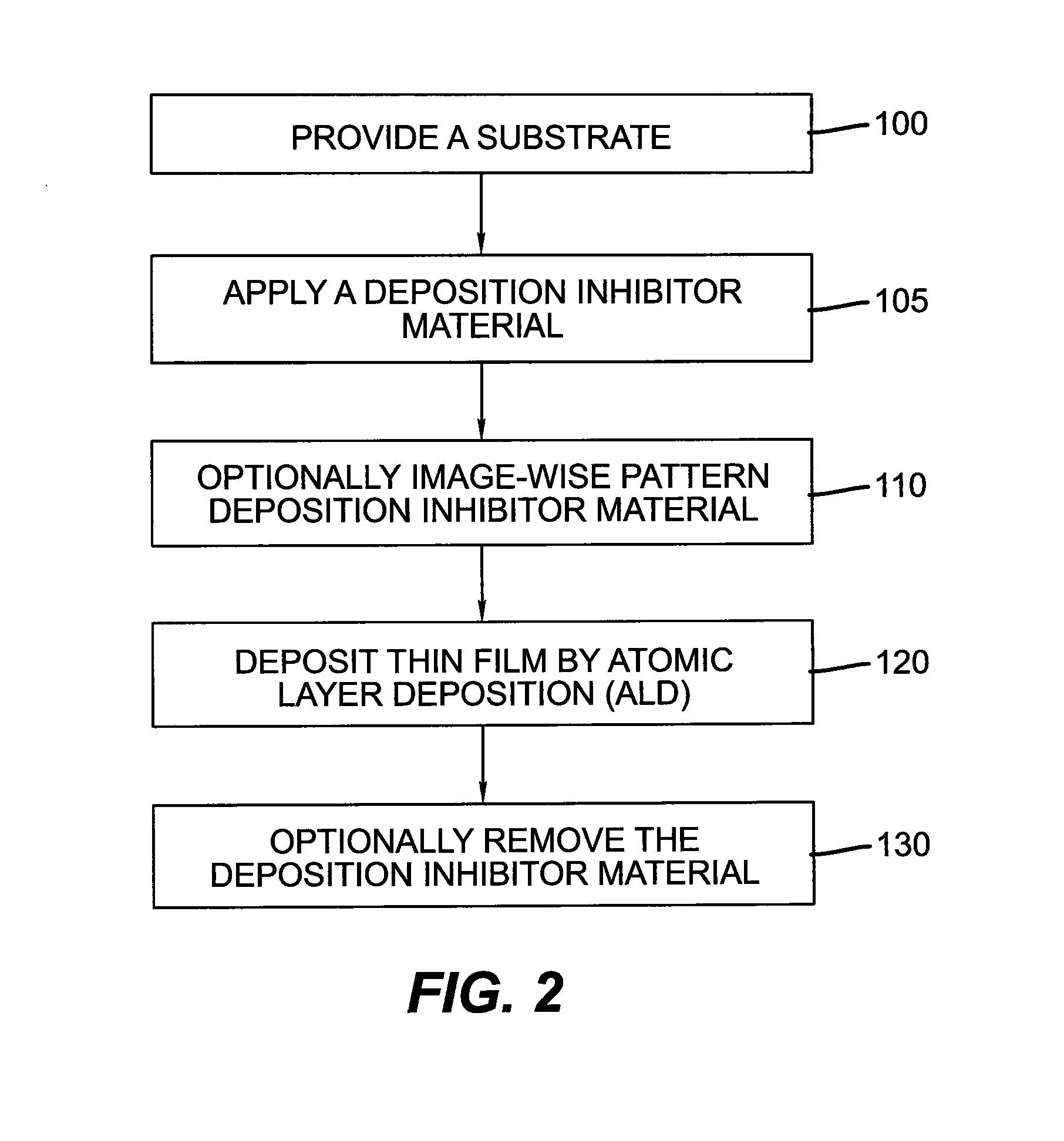
Method of making electronic devices using selective deposition
a technology of selective deposition and electronic devices, applied in the direction of resistive material coating, nuclear engineering, railway components, etc., can solve the problems of limiting device processing to below 200° c, difficult to align transistor components across typical substrate widths up to one meter or more, and traditional photolithographic processes and equipment can be seriously impacted, so as to achieve the effect of easy re-reform
- Summary
- Abstract
- Description
- Claims
- Application Information
AI Technical Summary
Benefits of technology
Problems solved by technology
Method used
Image

Examples
invention example 1
Thermal Transfer Patterning
[0197]To demonstrate laser thermal patterning using cyanoacrylate polymer inhibitors, a donor element was prepared in the following manner:
[0198]A 2.5 inch (6.35 cm) by 2.5 inch (6.35 cm) clean glass substrate was coated with 700 Å of chromium by thermal evaporation to form a light absorbing layer. An array of standoff spacers was created by spin coating a solution of Novolac resin, crystal violet, and an infrared radiation dye (IR Dye 1) onto the chromium surface and baking the resulting thermal resist at 230° C. for 7 minutes. The thermal resist was exposed with a computer-controlled laser imager having an array of 256 individually addressable 830 nm spots, each about 2.5 μm, focused on the image surface and scanned in swaths about 0.6 mm wide at a rate of 0.4 m / sec. The resulting pattern was an array of unexposed rectangles surrounded by areas having been exposed to 0.6 g / cm2. The exposed element was then developed using Goldstar Plus lithographic devel...
invention example 2
Reusable Donor Element for Thermal Transfer
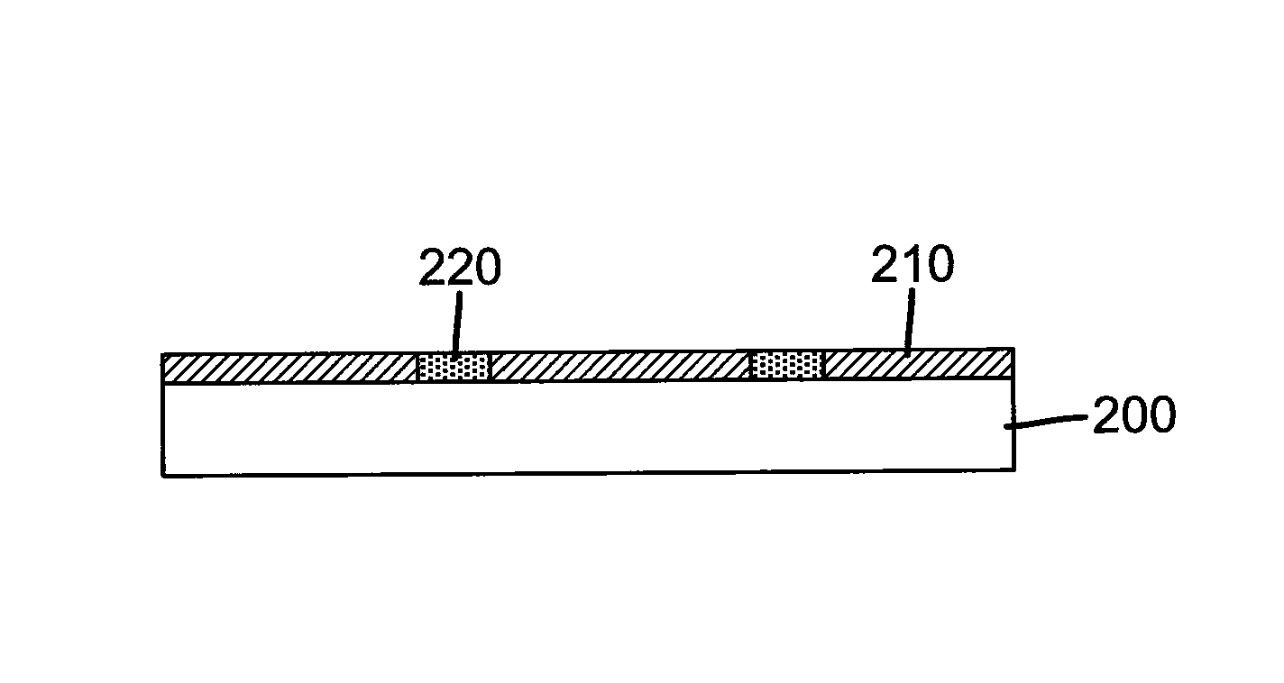
[0200]The ability to reuse a donor element was demonstrated by washing an exposed donor as described in Invention Example 1 in acetone and isopropyl alcohol, drying, and then spinning a new layer of a 7.5 weight % solution of poly(ethylmethyl cyanoacrylate) in 1:1 acetonitrile and cyclopentanone at 6,000 rpm on the substrate surface. It was observed that washing and recoating the substrate left the novolac spacers intact. The coated donor element was again placed coated side up on the laser imager and a clean glass substrate (receiver element) was affixed on top. The assembly of donor element and receiver element was then exposed as before with 2.5 J / cm2. The cyanoacrylate polymer inhibitor was transferred to the receiver element only in the exposed areas leaving the non-exposed squares on the receiver element unaffected. The receiver element was then subjected to 176 cycles of diethylzinc and water at 150° C. substrate temperature. Deposit...
PUM
| Property | Measurement | Unit |
|---|---|---|
| thickness | aaaaa | aaaaa |
| thickness | aaaaa | aaaaa |
| thickness | aaaaa | aaaaa |
Abstract
Description
Claims
Application Information