Group VA-doped solution-processed metal chalcogenides

Inactive Publication Date: 2014-04-01
SHARP KK
View PDF5 Cites 3 Cited by
  • Summary
  • Abstract
  • Description
  • Claims
  • Application Information

AI Technical Summary

Benefits of technology

The patent describes a method for making a high-quality antimony-doped CIGS absorber layer using a solution-based approach. The method involves depositing a precursor film of copper, indium, gallium, and selenium onto a conductive substrate, and then subjecting it to a thermal annealing process in the presence of selenium. The resulting layer has improved performance and morphology compared to traditional vacuum and electrodeposition methods. The method can be carried out using hydrazine-based solvents or low-boiling alcohols or acids. The use of antimony as a dopant in CIGS has been shown to improve performance, and the method described herein offers a safer alternative to hydrazine. The patent also describes a method for making a Group VA-doped metal chalcogenide layer by depositing a precursor film and then subjecting it to a thermal annealing process in the presence of selenium. The method can be carried out using various first material groups, such as aluminum, antimony, arsenic, bismuth, cadmium, chromium, cobalt, copper, gallium, germanium, gold, iron, lead, manganese, mercury, molybdenum, nickel, niobium, osmium, palladium, platinum, rhodium, ruthenium, silver, tantalum, tin, titanium, tungsten, vanadium, zinc, zirconium, and combinations thereof.

Problems solved by technology

As mentioned the Background Section above, solution-processed approaches to CIGS absorber layer fabrication have historically demonstrated lower performances relative to vacuum and electrodeposition methods.
Unfortunately, the hazards associated with hydrazine may limit the practical application of such approaches in manufacturing capacities.

Method used


Image

  • Group VA-doped solution-processed metal chalcogenides
  • Group VA-doped solution-processed metal chalcogenides
  • Group VA-doped solution-processed metal chalcogenides

Examples


Embodiment Construction

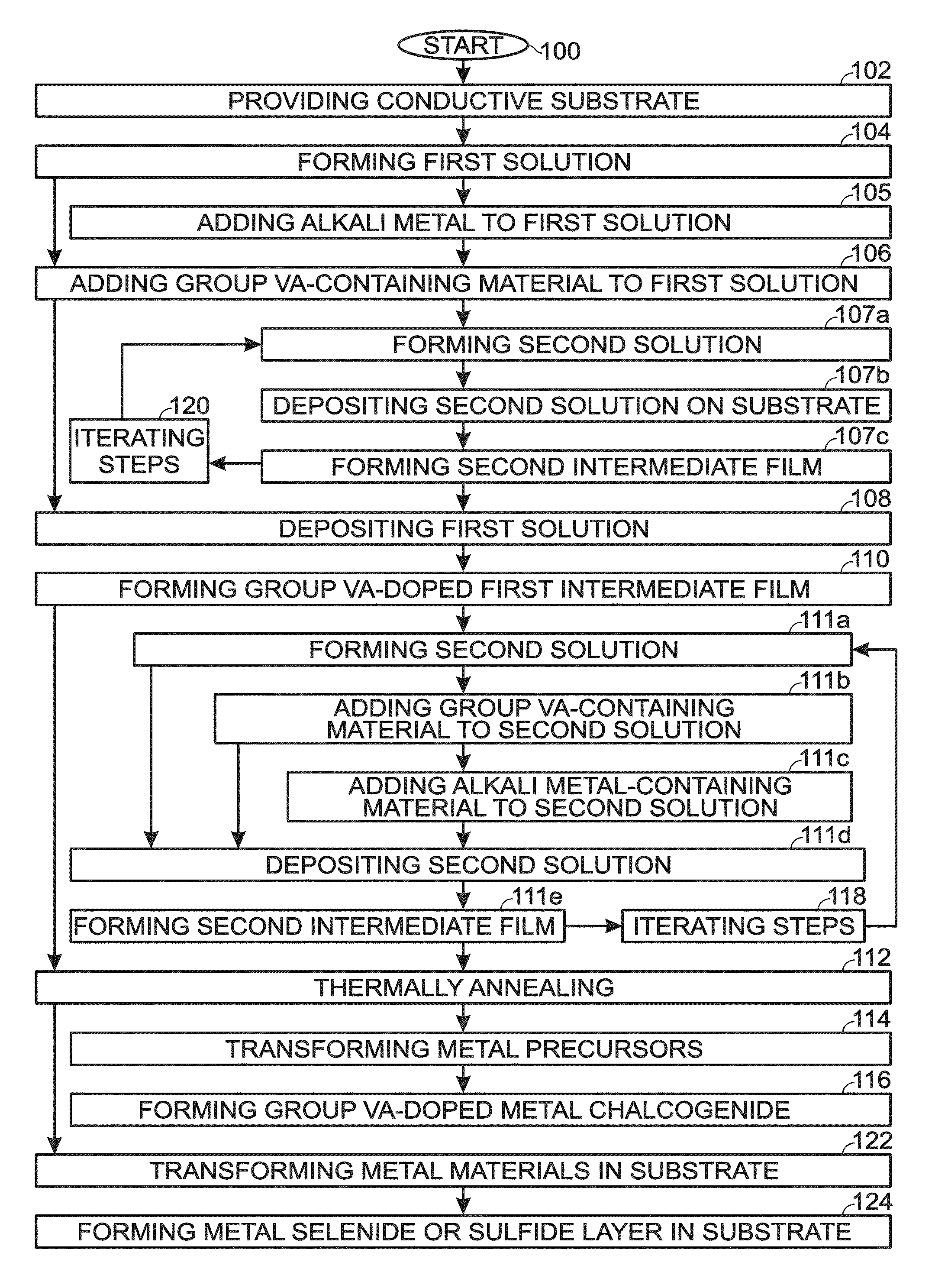
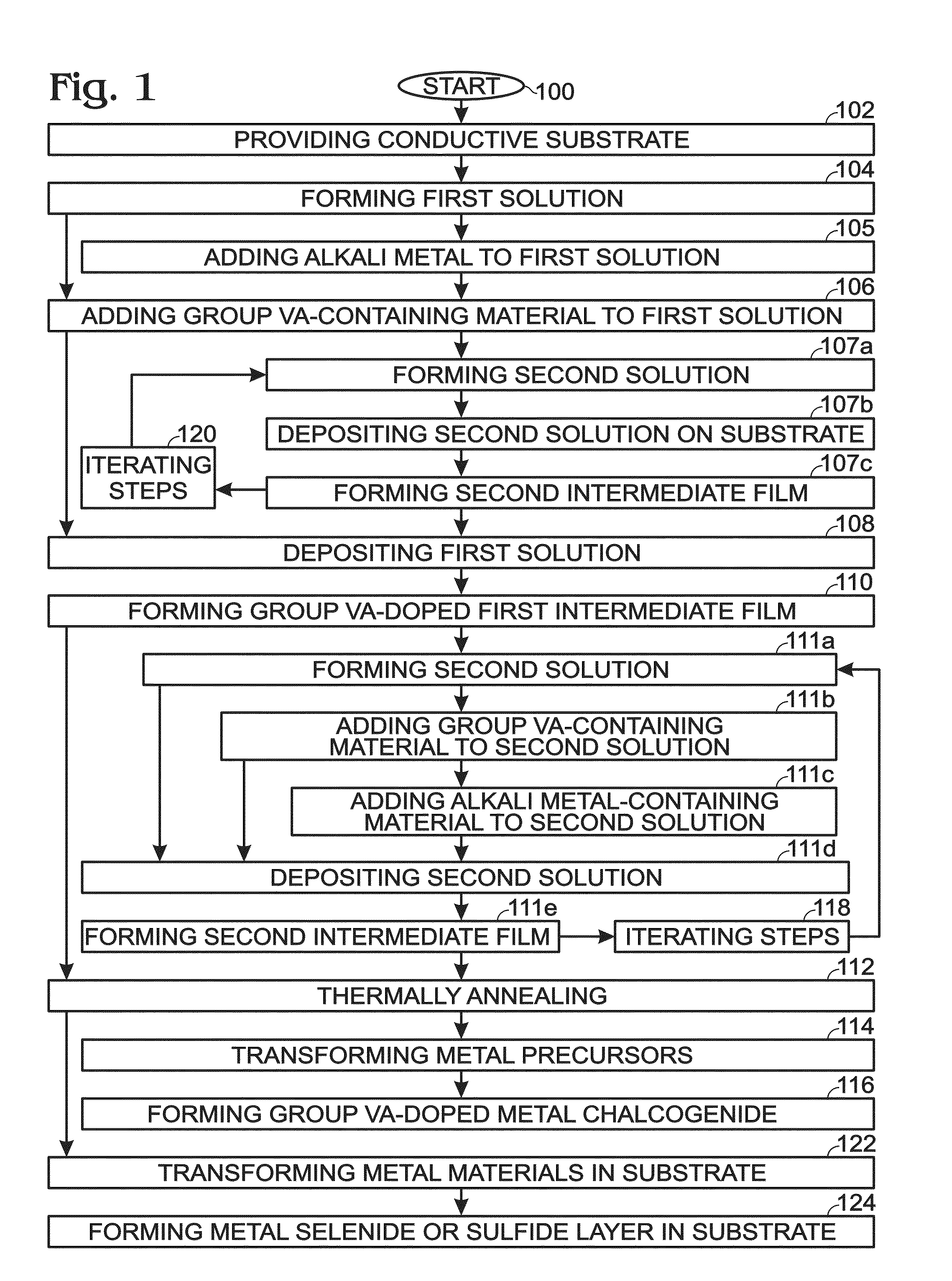
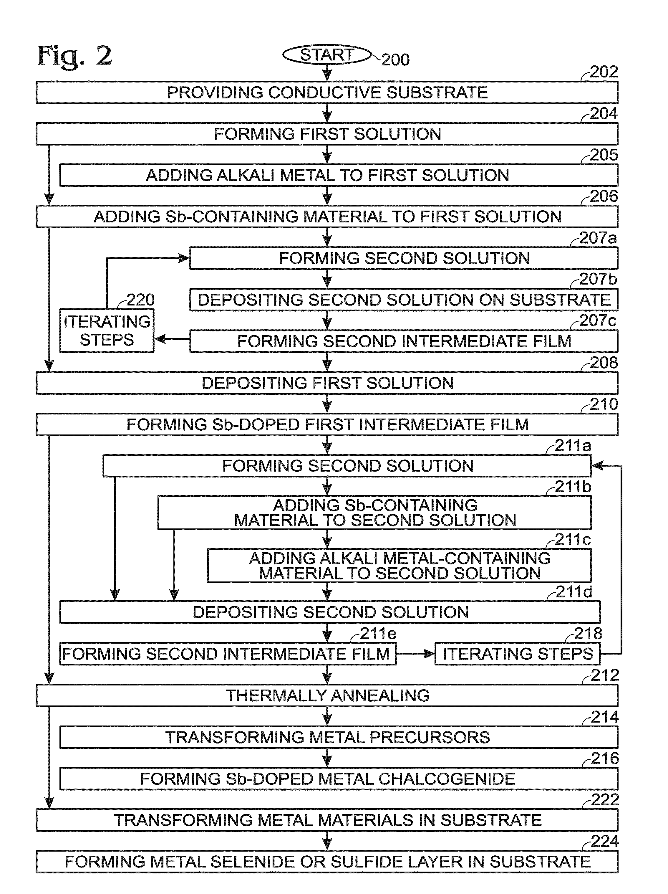
[0040]FIG. 1 is a flowchart illustrating a method for forming a Group VA-doped solution-processed metal chalcogenide. Although the method is depicted as a sequence of numbered steps for clarity, the numbering does not necessarily dictate the order of the steps. It should be understood that some of these steps may be skipped, performed in parallel, or performed without the requirement of maintaining a strict order of sequence. Generally however, the method follows the numeric order of the depicted steps. The method begins at Step 100.

[0041]Step 102 provides a conductive substrate. The conductive substrate may be a metal, metal alloy, metal oxide, mixed metal oxide, or a combination thereof. Some examples of conductive substrate materials include aluminum, chromium, cobalt, copper, gallium, germanium, gold, indium, iron, lead, molybdenum, nickel, niobium, palladium, platinum, silicon, silver, tantalum, tin, titanium, tungsten, vanadium, zinc, zirconium, stainless steel, indium tin oxi...


PUM


Abstract

A method is provided for forming a Group VA-doped solution-processed metal chalcogenide. The method forms a first solution including a first material group, dissolved in solvent. A Group VA-containing material is added to the first solution. The Group VA-containing material may include arsenic (As), antimony (Sb), bismuth (Bi), or combinations thereof. The first solution is deposited on a conductive substrate, and a Group VA-doped first intermediate film is formed comprising metal precursors from corresponding members of the first material group. Thermal annealing is performed in an environment of selenium (Se), Se and hydrogen (H2), hydrogen selenide (H2Se), sulfur (S), S and H2, hydrogen sulfide (H2S), or combinations thereof. As a result, the metal precursors in the Group VA-doped first intermediate film are transformed, forming a Group VA-doped metal chalcogenide layer. In one aspect, an antimony-doped Cu—In—Ga—Se chalcogenide (CIGS) is formed.

Description

RELATED APPLICATION[0001]The application is a Continuation-in-Part of an application entitled, ALKALI METAL-DOPED SOLUTION-PROCESSED METAL CHALCOGENIDES, invented by Sean Vail et al., Ser. No. 13 / 773,283, filed on Feb. 21, 2013;[0002]which is a Continuation-in-Part of an application entitled, SOLUTION-PROCESSED METAL SELENIDE SEMICONDUCTOR USING DEPOSITED SELENIUM FILM, invented by Sean Vail et al., Ser. No. 13 / 719,052, filed on Dec. 18, 2012;[0003]which is a Continuation-in-Part of an application entitled, ELECTROCHEMICAL SYNTHESIS OF SELENIUM NANOPARTICLES, invented by Wei Pan et al., Ser. No. 13 / 711,356, filed on Dec. 11, 2012;[0004]which is a Continuation-in-Part of an application entitled, SOLUTION-PROCESSED METAL SELENIDE SEMICONDUCTOR USING SELENIUM NANOPARTICLES, invented by Sean Vail et al., Ser. No. 13 / 674,005, filed on Nov. 10, 2012. The above-mentioned applications are incorporated herein by reference.BACKGROUND OF THE INVENTION[0005]1. Field of the Invention[0006]This i...

Claims


Application Information

Patent Timeline
IPC IPC(8): H01L31/18
CPCY02E10/541H01L31/03928H01L31/18H01L31/0322
Inventor VAIL, SEANKOPOSOV, ALEXEYFOLEY, GARY
Owner SHARP KK
Why Eureka
Try Eureka