Plating method of circuit substrate, production method of plated circuit substrate, and silver etching liquid

a technology of circuit substrate and silver etching liquid, which is applied in the direction of liquid/solution decomposition chemical coating, conductive pattern formation, coating, etc., can solve the problems of difficult to achieve high bonding strength (adhesion strength) of the metal layer by post-firing method, and large amount of electric current. , to achieve the effect of improving the yield, enhancing the corrosion resistance of the conductive pattern, and enhancing the adhesion strength

Inactive Publication Date: 2015-04-28
TOKUYAMA CORP
View PDF12 Cites 4 Cited by
  • Summary
  • Abstract
  • Description
  • Claims
  • Application Information

AI Technical Summary

Benefits of technology

[0026]With the plating method of a circuit substrate according to the first aspect of the present invention, when performing plating on a circuit substrate having a conductive pattern in which a metal layer containing at least silver and copper is exposed on the outer surface, it is possible to inhibit plating deposition on a part other than the conductive pattern part, and to form a favorable plating layer on the surface of the conductive pattern. Thus, the yield can be improved.
[0027]In the first aspect of the present invention, the step (D) comprises the above step (D1) and the above step (D2) in this mentioned order, thereby enabling corrosion resistance of the conductive pattern to be enhanced by the presence of the noble metal plating layer. Further, since noble metal to constitute the noble metal plating layer, which is the topmost layer, can be selected adequately as needed, the compatibility with a solder, a bonding wire and the like to be used for mounting an electronic component can be easily improved. Furthermore, with the presence of the nickel plating layer, it is possible to easily enhance the adhesion strength of the noble metal plating layer, to adjust firmness of the conductive pattern, and to prevent migration of copper toward the surface layer.
[0028]In the first aspect of the present invention, an aqueous solution containing one or more selected from permanganates and bichromates is employed as the first liquid agent; thereby plating deposition on the part other than the conductive pattern part can be easily inhibited.
[0029]In the first aspect of the present invention, an aqueous solution containing sulfuric acid and hydrogen peroxide is employed as the second liquid agent; thereby a favorable plating layer can be formed on the surface of the conductive pattern.
[0030]In the first aspect of the present invention, an aqueous solution containing hydrogen peroxide and ammonia is employed as the third liquid agent; thereby a favorable plating layer can be formed on the surface of the conductive pattern.
[0031]In the first aspect of the present invention, a liquid agent which dissolves silver oxide (I) at 25° C. at a rate 2500 times or more faster than a rate of dissolving copper (0) at 25° C. is employed as the third liquid agent; thereby a favorable plating layer can be formed on the surface of the conductive pattern even more easily.

Problems solved by technology

Especially in the uses where the heat radiating capability is required, a large amount of electric current is often needed.
The co-firing method has characteristics that although it enables a solidly adhered metal layer to be formed, it causes difficulty in forming a metal pattern with high dimensional precision due to the shrinkage of the ceramic that results from the sintering thereof.
However, especially in the nitride ceramics, a typical example of which is aluminum nitride, it has been difficult to attain high bonding strength (adhesion strength) of the metal layer by the post-firing method.

Method used


Image

  • Plating method of circuit substrate, production method of plated circuit substrate, and silver etching liquid
  • Plating method of circuit substrate, production method of plated circuit substrate, and silver etching liquid
  • Plating method of circuit substrate, production method of plated circuit substrate, and silver etching liquid

Examples


example 1

Preparation of First Paste Composition

[0173]A mortar was used to pre-mix 15 parts by mass of copper powder having an average particle size of 0.3 μm, 82 parts by mass of copper powder having an average particle size of 2 μm, and 3 parts by mass of titanium hydride powder having an average particle size of 5 μm, with a vehicle in which polyalkyl methacrylate was dissolved in terpineol; and thereafter a three-roll mill was used to subject the mixture to a dispersion treatment, thereby preparing a first paste composition.

Preparation of Second Paste Composition

[0174]A mortar was used to pre-mix Ag—Cu alloy powder (BAg-8; composition: 72 weight % of silver-28 weight % of the copper) having an average particle size of 6 μm, with a vehicle in which polyalkyl methacrylate was dissolved in terpineol; and thereafter a three-roll mill was used to subject the mixture to a dispersion treatment, thereby preparing a second paste composition.

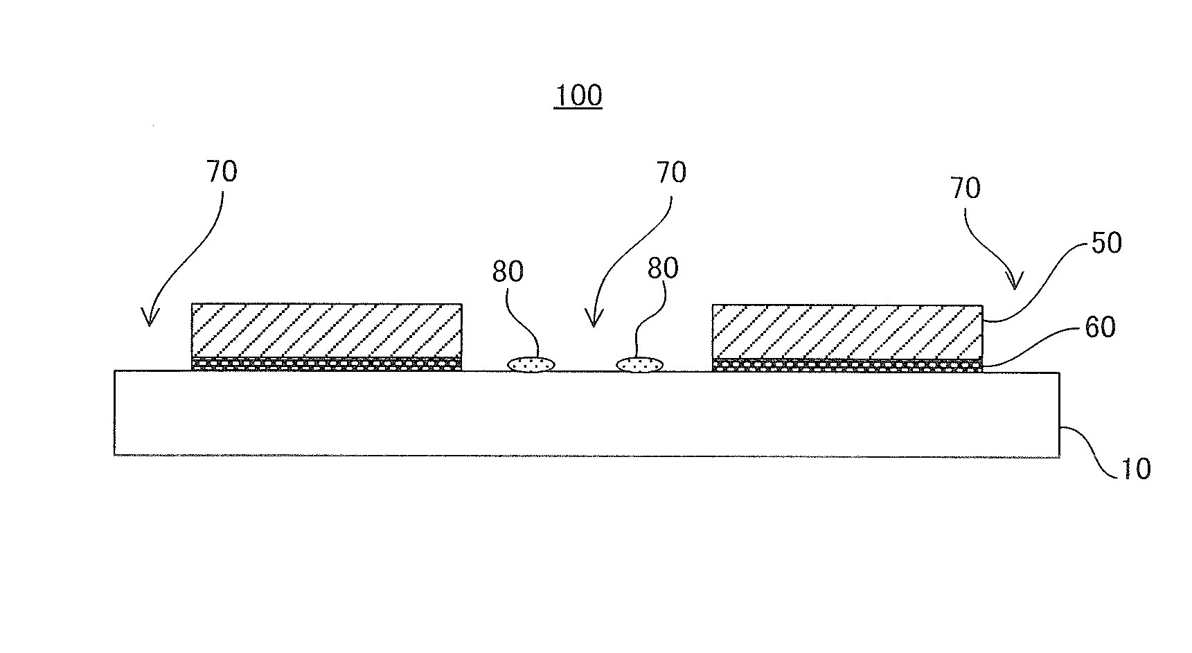
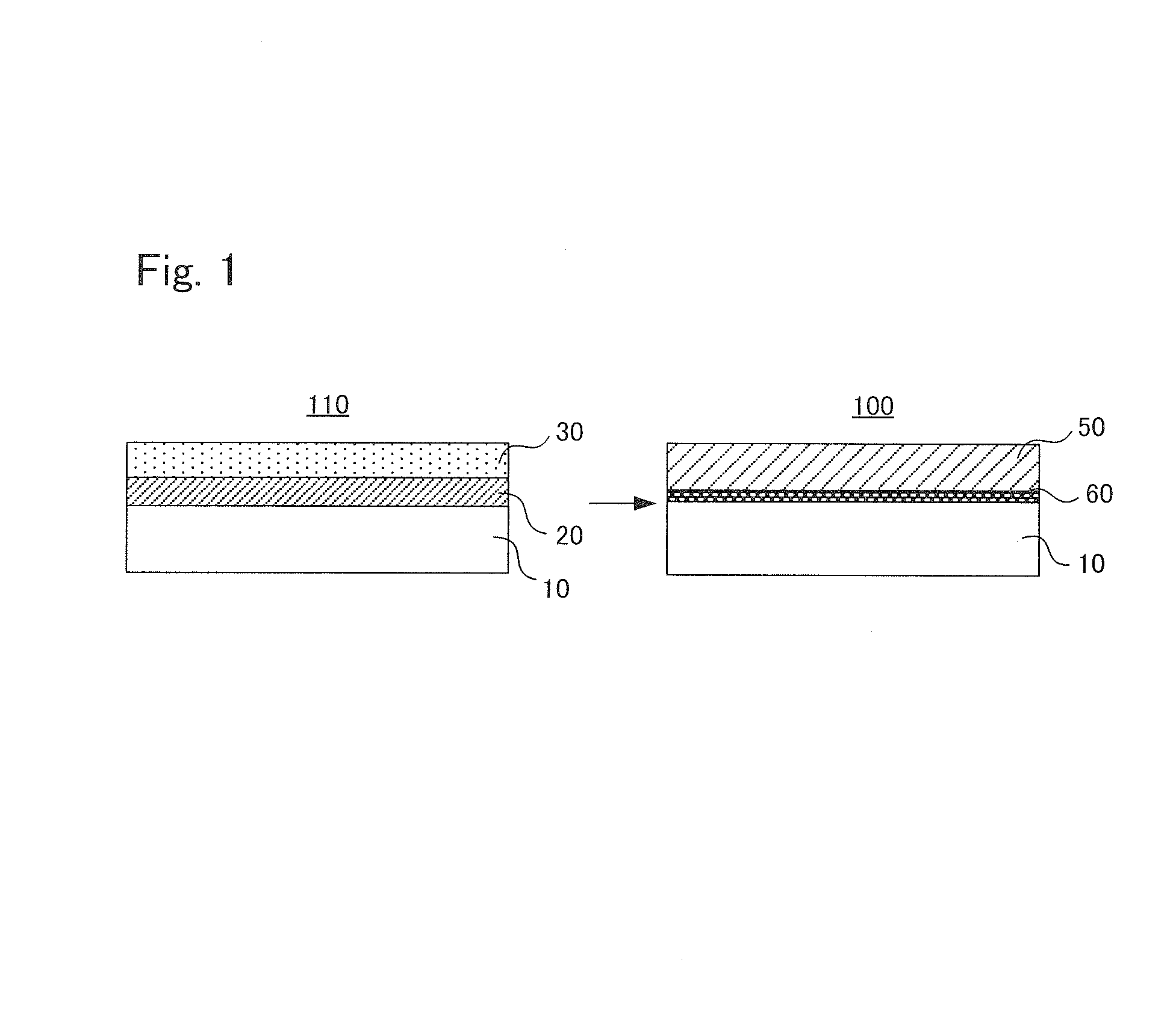
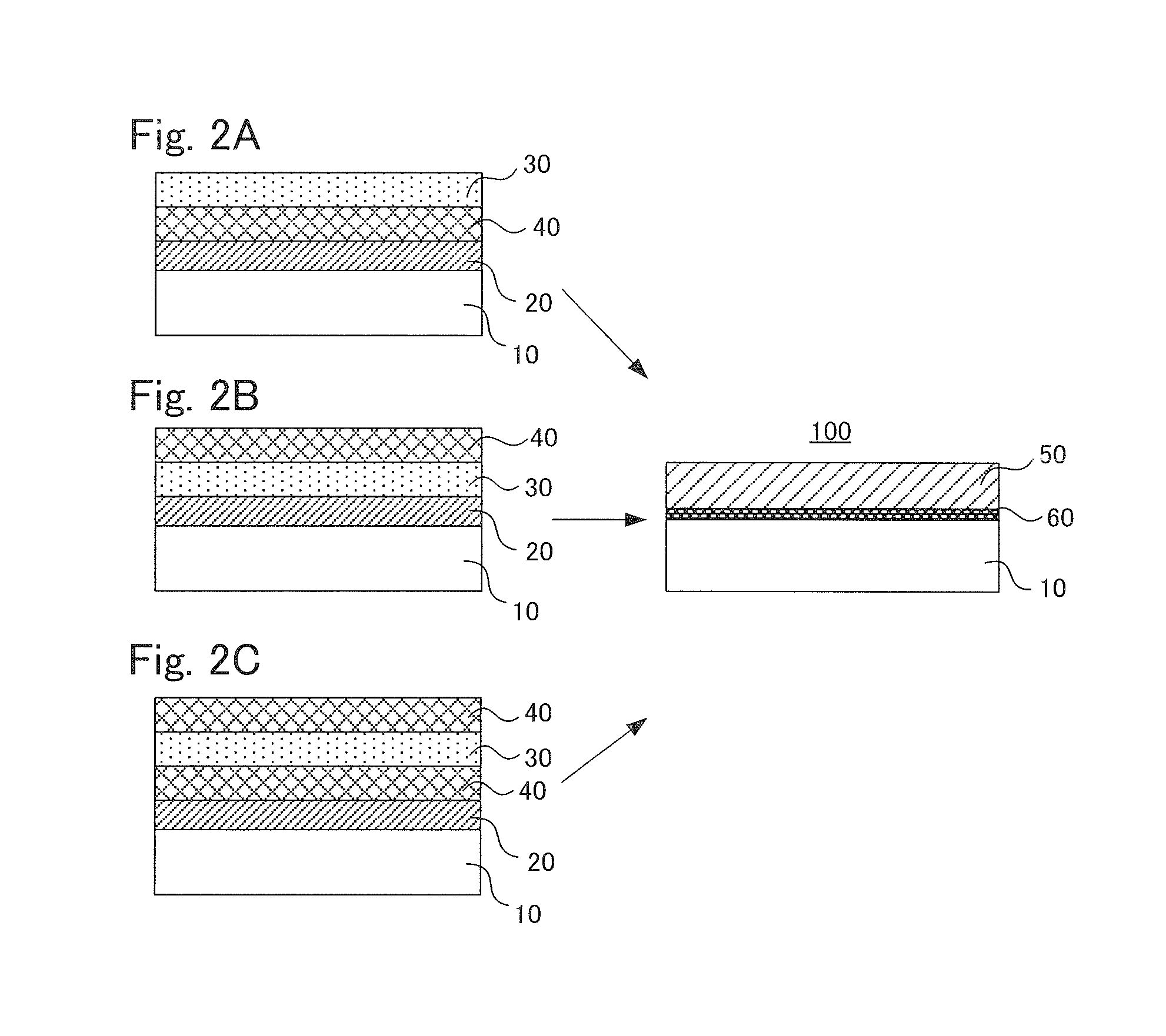
[0175](Production of Metallized Ceramic Circuit Substrate...

examples 2 to 5

, Comparative Examples 11 to 13

[0220]A test on the silver etching liquid according to the third aspect of the present invention was conducted by the following procedures.

[0221](Evaluation Method)

[0222]A liquid in which 1 mass % of phosphoric acid was dissolved in 20 mass % of hydrogen peroxide was prepared. Thereafter, 30 mass % of ammonia water was added thereto so that the pH becomes as shown in Table 2; thereby an etching liquid was prepared. The etching liquid was kept at 25° C., and a copper plate and an oxidized silver plate (which was heated at 300° C. in the atmosphere for 60 minutes) were immersed into the etching liquid and etched. The concentrations of the copper and the silver in the etching liquid after etching were measured by ICP emission spectrometry; and the results were converted into an etching rate (dissolution rate). The results are shown in Table 2.

[0223]

TABLE 2Rate ofRate of dissolvingRate of dissolvingdissolvingsilver oxide (I) / silver oxide (I)copper (0)Rate ...


PUM

PropertyMeasurementUnit
viscosityaaaaaaaaaa
temperatureaaaaaaaaaa
thicknessaaaaaaaaaa

Abstract

Provided is a plating method of a circuit substrate comprising a conductive pattern in which a metal layer containing at least silver and copper is exposed on an outer surface. The plating method comprises: step (A) of treating the circuit substrate with a first liquid agent containing an oxidizing agent; step (B) of treating the circuit substrate after the step (A) with a second liquid agent which dissolves copper oxide, and thereby removing copper oxide from the conductive pattern's surface; step (C) of treating the circuit substrate after the step (B) with a third liquid agent whose rate of dissolving silver oxide (I) at 25° C. is 1000 times or more faster than its rate of dissolving copper (0) at 25° C., and thereby removing silver oxide from the conductive pattern's surface; and step (D) of performing electroless plating on the conductive pattern of the circuit substrate after the step (C).

Description

TECHNICAL FIELD[0001]The present invention relates to a circuit substrate for mounting thereon an electronic component such as a semiconductor device. More specifically, it relates to a plating method of a circuit substrate, a production method of a plated circuit substrate, and a silver etching liquid.BACKGROUND ART[0002]An electronic component such as a semiconductor device is usually mounted on a circuit substrate. In general, the circuit substrate comprises an insulating base material and a conductive pattern. Examples of the insulating base material that can be used in the circuit substrate not only include: resin materials such as Bakelite; impregnation materials such as a paper phenol material made by hardening paper with a phenolic resin, and a glass epoxy material made by hardening glass fiber with an epoxy resin; but also include ceramics and glass.[0003]The amount of heat generated by an electronic component, especially a semiconductor device, to be mounted onto a circuit...

Claims


Application Information

Patent Timeline
Patent Type & Authority Patents(United States)
IPC IPC(8): H01B13/00C03C15/00C25D5/54H01L21/30C09K13/00C23C18/12C23C18/16C23C18/18C23C22/52C23C22/63C23G1/10C23G1/20H05K1/03H05K3/12H05K3/24
CPCC23G1/103C23C22/52C23C22/63C23G1/20C23C18/1844C23C18/1216C23C18/1651H05K3/246H05K1/0306H05K3/1291H05K2203/0796
Inventor USHIODA, EMIIMAI, TETSUO
Owner TOKUYAMA CORP
Why Eureka
Try Eureka