Method and apparatus for in-situ monitoring of plasma etch and deposition processes using a pulsed broadband light source

a plasma etching and in-situ monitoring technology, applied in the field of semiconductor/solid-state device testing/measurement, instruments, vacuum evaporation coating, etc., can solve the problems of inconvenient in-situ monitoring of plasma etching and deposition processes, fluctuation of plasma emission can also confound models used to determine etching rate, and the method is not useful in several etching processes, etc., to reduce reducing the effect of plasma emission ratio ratio ratio

Inactive Publication Date: 2006-06-27
LAM RES CORP
View PDF8 Cites 8 Cited by
  • Summary
  • Abstract
  • Description
  • Claims
  • Application Information

AI Technical Summary

Benefits of technology

[0015]According to a first aspect of the invention, the apparatus includes a light source, a collimator, a light sensitive detector such as a spectrograph for monitoring an intensity from the light reflected from the wafer, the spectrograph being operable to disperse light into multiple wavelengths that are detected by multiple detectors, and a data processing element for processing the signal from the spectrograph and estimating the thickness of any film on the substrate. The light source is preferably a flash lamp emitting a broadband, optical radiation synchronous with a data acquisition cycle of the spectrograph. Data are recorded only during the short output pulse from the flash lamp and the integration time of the spectrograph is thereby reduced. The background light received from the processing plasma is proportional to the integration time so the effect of the plasma emission on the spectrograph signal is largely eliminated.
[0016]According to a second aspect of the invention, plasma intensity is recorded while the flash lamp is off and the detected signal is subtracted from the signal recorded with the flash lamp on. This embodiment further reduces the effect of the plasma emission on the measurement.
[0017]According to a third aspect of the invention, the spectrograph comprises a multi-channel spectrograph. A channel of the spectrograph is utilized to monitor the flash lamp signal on each pulse. Variations in the flash lamp signal are removed from the signal to reduce variations in the interferometer signal.

Problems solved by technology

This method is not useful however in several etch processes where an underlying film is not exposed.
Spectroscopy is also not useful in shallow trench isolation and recess etch processes.
Fluctuations in the plasma emission can also confound models used to determine the etch rate of films on the wafer.
The use of laser interferometry greatly reduces sensitivity to plasma emission but limits measurement to a single wavelength.
Methods using extended broadband light sources provide a range of wavelengths useful for analysis but generally suffer from problems of low signal to noise ratio and low intensity interferometric signals.
Prior art ultraviolet light sources are typically extended sources and coupling light efficiently from these sources is optically difficult.
Finally these sources typically have relatively low intensity thereby making the interferometric signal harder to detect above the plasma emission background.

Method used


Image

  • Method and apparatus for in-situ monitoring of plasma etch and deposition processes using a pulsed broadband light source
  • Method and apparatus for in-situ monitoring of plasma etch and deposition processes using a pulsed broadband light source
  • Method and apparatus for in-situ monitoring of plasma etch and deposition processes using a pulsed broadband light source

Examples


Embodiment Construction

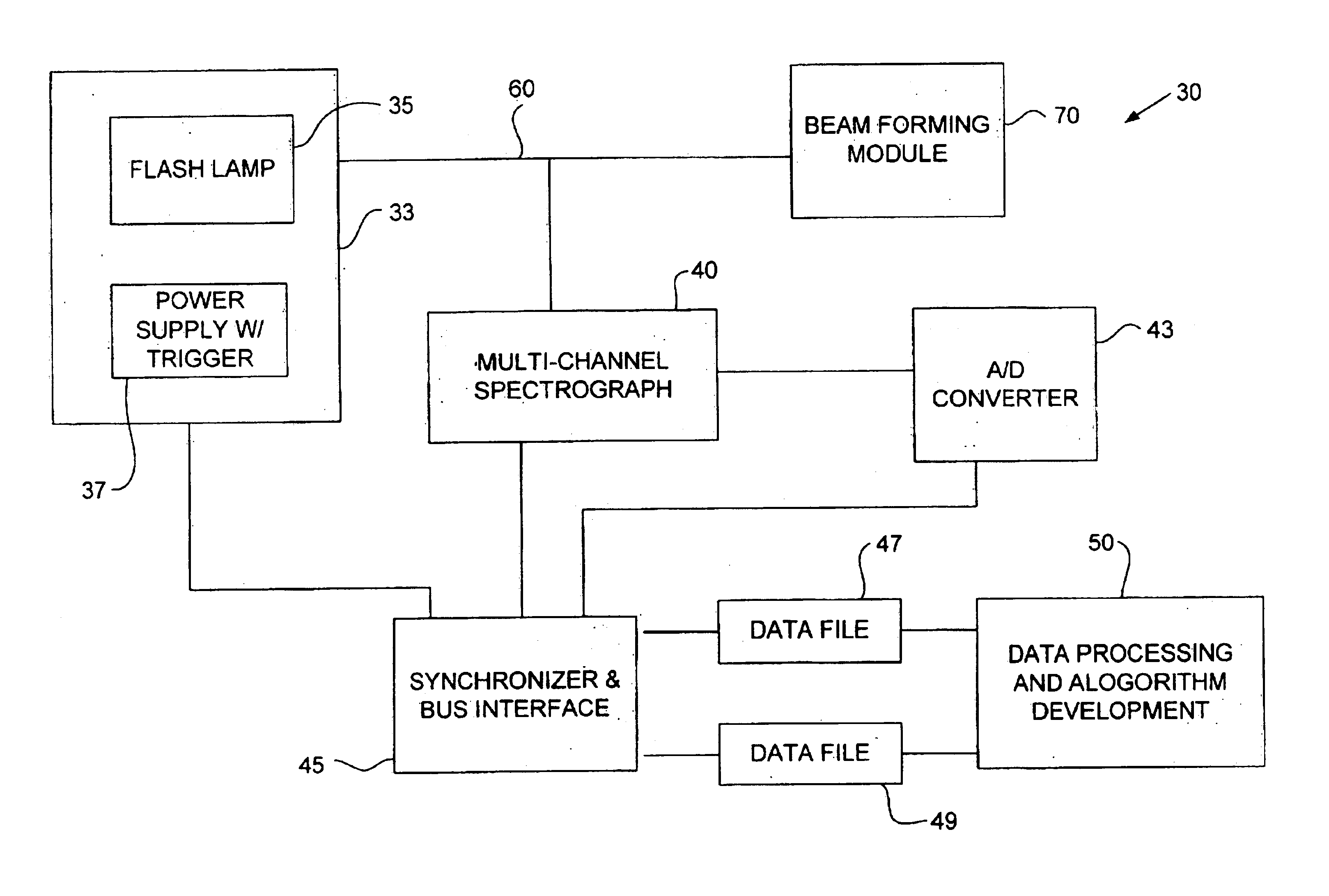
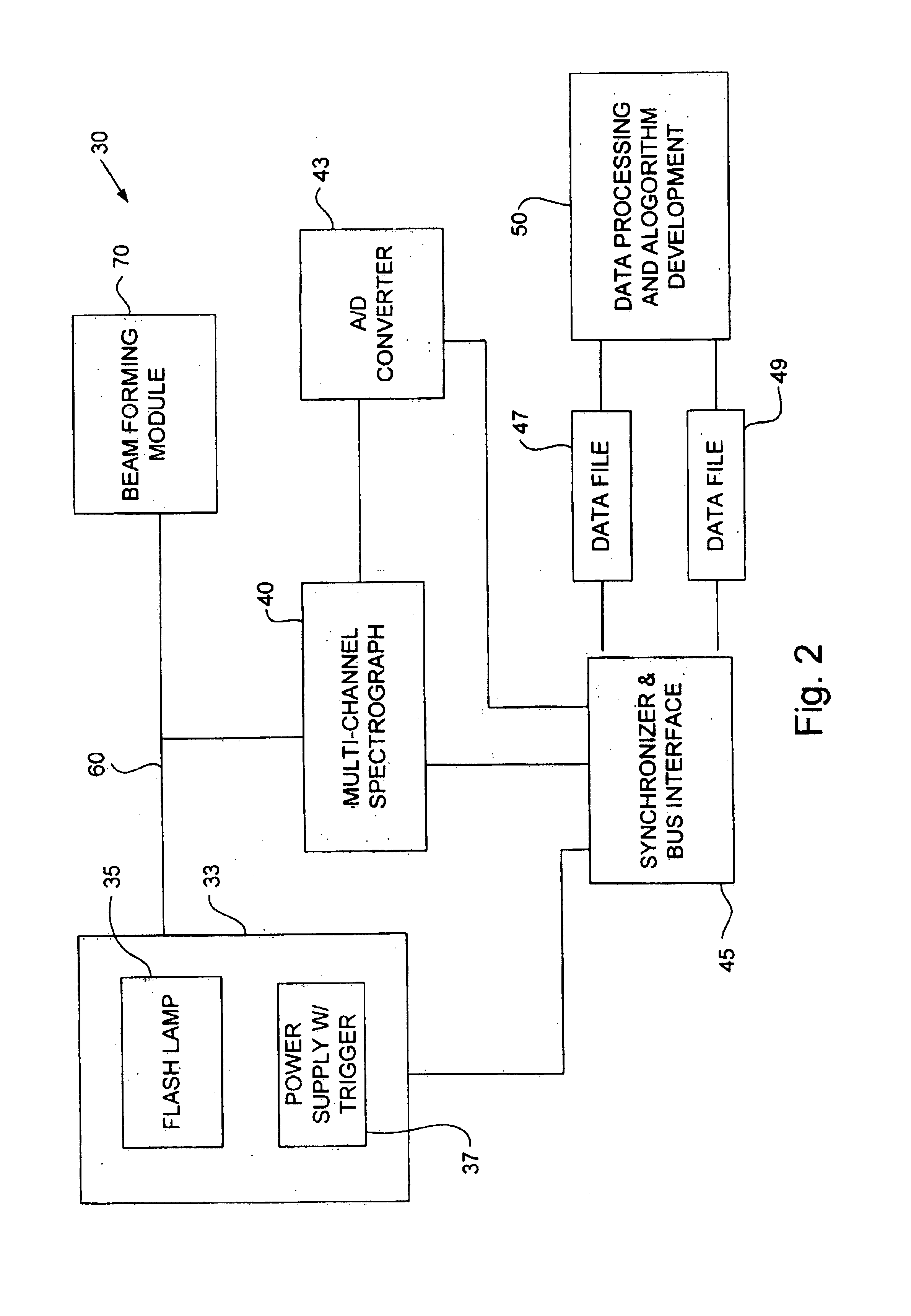
[0023]FIG. 2 shows the components of a system generally designated 30 using multiple wavelength illumination. The system 30 comprises an illumination module 33 comprising a flash lamp 35 and a power supply with trigger 37. The system 30 also comprises a multi-channel spectrograph 40, an analog-to-digital converter 43, a synchronizer and bus interface 45, a first and second data file 47 and 49 and a data processing and algorithm development block 50. An optical fiber 60 optically connects the flash lamp 35 and the spectrograph 40 to a beam forming module 70 disposed outside of a plasma chamber. This system 30 is used to calculate the thickness of a film on a wafer positioned within the plasma chamber, as described below.

[0024]The flash lamp 35 generates broadband light in the range of about 200 nm to 2 microns. The optical fiber 60 carries the broadband light from the flash lamp 35 to the beam forming module 70 disposed outside the plasma chamber. The beam forming module 70 includes ...


PUM

PropertyMeasurementUnit
optical radiationaaaaaaaaaa
thicknessaaaaaaaaaa
conductiveaaaaaaaaaa

Abstract

An interferometric method and apparatus for in-situ monitoring of a thin film thickness and of etch and deposition rates using a pulsed flash lamp providing a high instantaneous power pulse and having a wide spectral width. The optical path between the flash lamp and a spectrograph used for detecting light reflected from a wafer is substantially transmissive to the ultraviolet range of the spectrum making available to the software algorithms operable to calculate film thickness and etch and deposition rates desirable wavelengths.

Description

BACKGROUND OF THE INVENTION[0001]The present invention relates to the field of semiconductor substrate processing and, more particularly, to the monitoring of material thickness and etch and deposition rates during plasma etch and deposition processes of semiconductor substrates.[0002]The manufacture of an integrated circuit device requires the formation of various layers (both conductive, semiconductive, and non-conductive) above a base substrate to form necessary components and interconnects. During the manufacturing process, removal of a certain layer or portions of layers must be achieved in order to form the various components and interconnects. This is commonly accomplished by means of an etching process. Etching techniques in use include wet, or chemical etching, and dry, or plasma etching. The latter technique is typically dependent upon the generation of reactive species from process gases that are impinged on the surface of the material to be etched. A chemical reaction ta...

Claims


Application Information

Patent Timeline
Patent Type & Authority Patents(United States)
IPC IPC(8): G01B11/06C23C14/54C23C16/52H01L21/205H01L21/3065
CPCG01B11/0683H01L22/00
Inventor PERRY, ANDREWMUNDT, RANDALL
Owner LAM RES CORP
Why Eureka
Try Eureka