

Preparation method of cadmium sulfide/silicon heterostructure with white light transmission
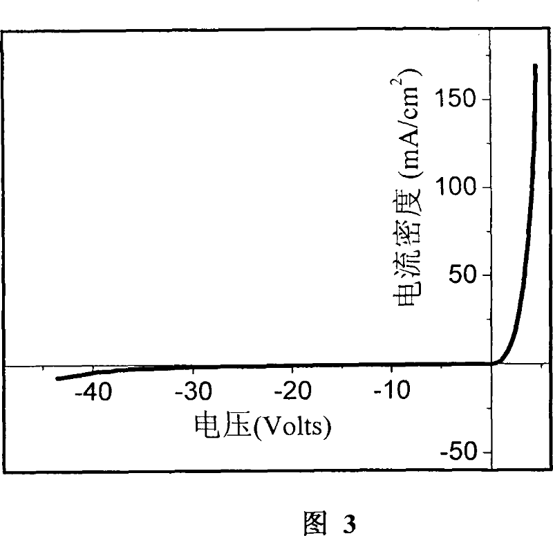
A heterostructure, cadmium sulfide technology, applied in the field of semiconductors, can solve the problems of non-adjustable luminescence peak position, single luminescence peak position, poor rectification characteristics, etc., and achieve the effect of good application prospects.
- Summary
- Abstract
- Description
- Claims
- Application Information
AI Technical Summary
Problems solved by technology
Method used
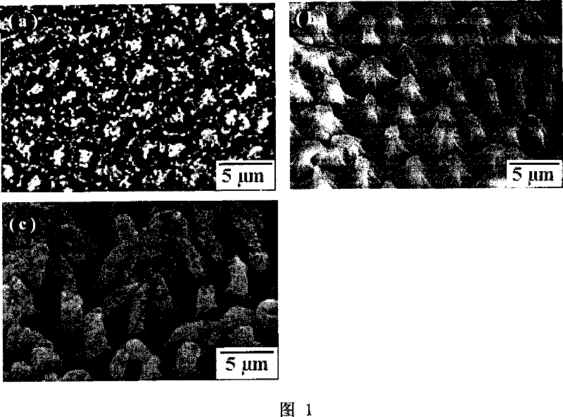
Image

Examples
Embodiment 1
[0019] 1. Put a P-type (111) oriented single crystal silicon wafer with a resistivity of 0.015Ω·cm into an autoclave, and fill it with a hydrofluoric acid solution with a concentration of 8.00mol / l and an aqueous ferric nitrate solution of 0.04mol / l. Etching solution, the solution volume filling degree of the autoclave is 95%, and it is etched at a temperature of 200 ° C for 30 minutes to prepare the substrate material silicon nanoporous column array (Si-NPA);
[0020] 2. Put the Si-NPA substrate into 0.005mol / l CdCl 2 Immerse in deionized aqueous solution for 30 hours, take it out and dry it naturally in the air at room temperature, put hydrogen sulfide (H 2 S) in-situ heterogeneous chemical reaction growth under natural conditions in air flow for 30 hours;
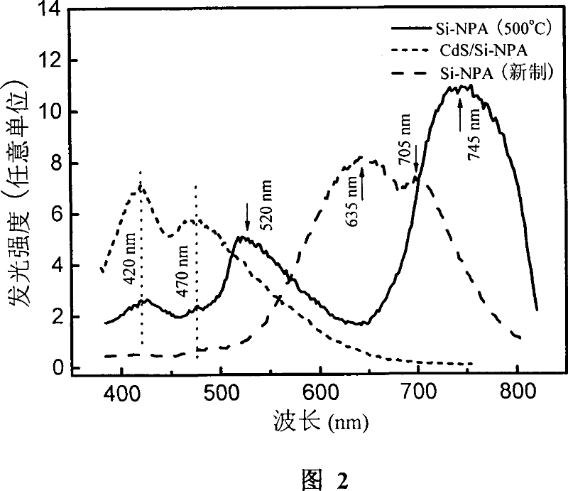
[0021] 3. After annealing at 100°C for 30 minutes in a high-purity nitrogen atmosphere, CdS nanorings and nanoparticles are formed at the bottom and top of each silicon column to form a CdS / Si heterostructure. Its morp...
Embodiment 2
[0023] 1. Put a P-type (111)-oriented single crystal silicon wafer with a resistivity of 0.10Ω·cm into an autoclave, and fill it with a hydrofluoric acid solution with a concentration of 17.00mol / l and an aqueous ferric nitrate solution of 0.25mol / l. Etching solution, the solution volume filling degree of the autoclave is 60%, corroding at a temperature of 60° C. for 16 hours, and preparing the substrate material silicon nanoporous column array (Si-NPA);
[0024] 2. Put the Si-NPA substrate into 1.0mol / l Cd(CH 3 COOH) 2 Immerse in 95% alcohol solution for 12 hours, take it out and dry it naturally in the air at room temperature, put it in hydrogen sulfide (H 2 S) in-situ heterogeneous chemical reaction growth under natural conditions in air flow for 12 hours;
[0025] 3. After annealing at 700°C for 10 minutes in an oxygen atmosphere, a "curtain"-like cadmium sulfide / silicon (CdS / Si) heterostructure can be obtained and white light emission with red, green and blue luminescen...
Embodiment 3
[0027] 1. Put a P-type (111) oriented single crystal silicon wafer with a resistivity of 2.80Ω·cm into an autoclave, and fill it with a hydrofluoric acid solution with a concentration of 22.00mol / l and an aqueous ferric nitrate solution of 0.5mol / l. Etching solution, the solution volume filling degree of the autoclave is 40%, and it is etched at a temperature of 50° C. for 35 hours to prepare the substrate material silicon nanoporous column array (Si-NPA);
[0028] 2. Put the Si-NPA substrate into Cd(NO 3 ) 2 Immerse in the methylene disulfone solution for 30 minutes, take it out, dry it naturally in the air at room temperature, put it in hydrogen sulfide (H 2 S) in-situ multi-phase chemical reaction growth under natural conditions in the air flow for 1 hour; and during the entire impregnation and in-situ growth process of the substrate, a columnar low-pressure mercury ultraviolet lamp with a power of 20W is used for irradiation induction;
[0029] 3. After annealing at 400°C ...
PUM
| Property | Measurement | Unit |
|---|---|---|
| Resistivity | aaaaa | aaaaa |
| Resistivity | aaaaa | aaaaa |
Abstract
Description
Claims
Application Information